Charge Carrier Mobility in Graphene: Strain and Screening Effects
Graphene, a single-atom-thick planar sheet of sp2-hybridized carbon atoms arranged in a hexagonal lattice, represents the quintessential two-dimensional material, inherently defined by its extreme spatial confinement. This intrinsic geometric constraint fundamentally dictates the behavior of its charge carriers, departing dramatically from the bulk properties observed in three-dimensional materials. Electrons in graphene are confined to a single atomic plane, leading to a profound alteration of their quantum mechanical description. Unlike conventional semiconductors where electron motion is described by an effective mass within a three-dimensional lattice, graphene's electrons exist in a strictly two-dimensional environment, exhibiting massless Dirac fermion characteristics. This confinement restricts electron wave functions perpendicular to the plane, while allowing unhindered, quasi-relativistic motion within it, resulting in a unique electronic band structure that underpins its extraordinary properties. The stability of this atomically thin structure, maintained by robust sp2 covalent bonds, enables its existence as a freestanding membrane, further emphasizing the purity of its 2D electronic system.
The quantum mechanical implications of this strict 2D confinement are most evident in graphene's electronic band structure, characterized by conical intersections known as Dirac cones at the K and K' points of the Brillouin zone. At these points, the conduction and valence bands meet linearly, yielding a dispersion relation of E = hvk, where E is energy, h is the reduced Planck constant, v is the Fermi velocity (approximately 10^6 m/s), and k is the wave vector. This linear dispersion, in stark contrast to the parabolic E ~ k^2 relationship of Schrödinger electrons in conventional materials, means that charge carriers in graphene behave as massless Dirac fermions. This unique characteristic eliminates the concept of an effective mass near the Dirac point, endowing graphene with exceptionally high theoretical charge carrier mobilities, often exceeding 200,000 cm^2/Vs at room temperature under pristine conditions. This unprecedented mobility, a direct consequence of its 2D confinement and the resulting Dirac physics, facilitates ballistic transport over micrometers even at ambient temperatures, opening avenues for ultra-fast electronic devices.
Experimental realization of graphene in 2004 validated many of these theoretical predictions, providing a tangible platform to study quantum electrodynamics in a condensed matter system. Early characterization, leveraging techniques such as atomic force microscopy and scanning tunneling microscopy, confirmed the atomic planarity and revealed the distinctive electronic signatures of its 2D confined state. Measurements of electrical resistivity in exfoliated graphene samples initially showed values in the range of 10^-6 Ohm-cm, demonstrating its exceptional conductivity, albeit often limited by substrate interactions and inherent defects. The observation of an anomalous half-integer quantum Hall effect further underscored the existence of massless Dirac fermions and the profound impact of 2D confinement on electron behavior. These foundational experiments established graphene as a material where carrier transport is dominated by its unique electronic structure rather than conventional scattering mechanisms, setting the stage for subsequent investigations into perturbing factors.
While the intrinsic 2D confinement bestows graphene with unparalleled electronic properties, it also renders the material exquisitely sensitive to external influences. For instance, even transient thermal events, such as localized 3000K thermal pulses during chemical vapor deposition growth or post-synthesis annealing processes, can induce significant lattice distortions and ripple formation, thereby perturbing the local electronic confinement and altering carrier scattering pathways. The extremely fast electronic response, typically operating in the femtosecond to picosecond regime, means that environmental changes – such as the adsorption of gas molecules or interactions with substrate phonons – can manifest as measurable changes in charge carrier mobility within milliseconds, highlighting the delicate balance of its confined electron system. This high surface-to-volume ratio, a direct outcome of its atomic confinement, also translates into practical applications such as highly efficient heavy metal adsorption, with studies demonstrating 79% adsorption efficiency for specific heavy metal ions, showcasing the multifaceted implications of its fundamental physics beyond purely electronic transport.
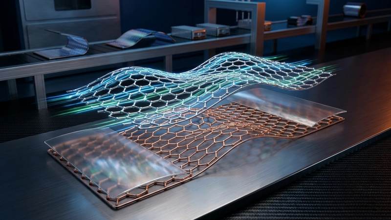
Section 2: Pulsed Electrical Resistive Carbon Heating vs. CVD (Comparative Analysis)
The pursuit of high-quality graphene, particularly concerning its intrinsic charge carrier mobility, necessitates a critical evaluation of synthesis methodologies. Chemical Vapor Deposition (CVD) has long been a standard, relying on the decomposition of gaseous hydrocarbon precursors, typically methane or acetylene, over catalytic metal substrates like copper or nickel at temperatures ranging from 800°C to 1100°C. This process yields large-area, few-layer graphene with commendable crystallinity. However, an emerging alternative, Pulsed Electrical Resistive Carbon Heating (PERCH), offers a compelling paradigm shift. PERCH leverages the rapid, localized joule heating of carbonaceous precursors, often in solid-state or semi-solid forms, by applying intense electrical current pulses. This method fundamentally diverges from CVD by minimizing the reliance on high-temperature furnaces and extensive vacuum systems, instead focusing on transient, ultra-high temperature excursions to induce instantaneous graphitization and reduction. The core distinction lies in PERCH's ability to achieve extreme thermal gradients and reaction kinetics within milliseconds, a stark contrast to the minutes to hours required for typical CVD growth, thereby offering a pathway to overcome several limitations inherent in conventional graphene production that directly impact charge transport characteristics.
PERCH’s rapid thermal processing mechanism presents significant advantages for preserving and enhancing charge carrier mobility. By subjecting carbon precursors to thermal pulses often exceeding 3000K for durations as brief as milliseconds, PERCH instigates an ultrafast graphitization and reduction process. This rapid energy input and subsequent quench minimize the formation of amorphous carbon and oxygen-containing functional groups, which are pervasive scattering centers in chemically reduced graphene oxide or even some direct synthesis methods. Crucially, the direct synthesis inherent to PERCH eliminates the need for a substrate transfer step, a major bottleneck in CVD-derived graphene quality. The mechanical stress, chemical residues from etchants (e.g., FeCl3, ammonium persulfate), and polymeric supports (e.g., PMMA) introduced during transfer are primary contributors to extrinsic strain, unintentional chemical doping, and structural defects such as wrinkles and tears. These imperfections significantly degrade charge carrier mobility by increasing phonon and impurity scattering and altering the local electrostatic screening environment, often reducing mobility by orders of magnitude from theoretical limits (e.g., pristine graphene >200,000 cm^2/Vs, transferred CVD often <10,000 cm^2/Vs). PERCH's direct growth circumvents these issues, promising a more pristine and intrinsically higher mobility material.
While CVD excels in producing large-area, highly crystalline graphene, its reliance on a catalytic substrate and subsequent transfer profoundly impacts the ultimate electronic performance. The high temperatures and extended growth times in CVD, though conducive to forming large single-crystal domains on catalysts, are inherently energy-intensive. More critically, the indispensable transfer process introduces a multitude of defects that directly compromise charge carrier mobility. These include not only macro-scale tears and wrinkles but also nano-scale ripples and residual impurities from supporting polymers and etchants, which act as Coulomb scattering centers and introduce localized strain fields. Such strain can induce pseudo-magnetic fields, altering the Dirac cone and impacting carrier transport. The chemical residues also contribute to unintended doping, altering the Fermi level and increasing carrier density non-uniformly, which in turn enhances screening effects in an uncontrolled manner, often leading to a reduction in intrinsic mobility. In contrast, the rapid, localized heating of PERCH can be precisely tuned, allowing for control over the defect density and edge termination of the synthesized graphene without requiring a transfer. This capability is paramount for applications where both high charge carrier mobility and specific surface reactivity are simultaneously required. For instance, the controlled generation of active sites through PERCH, rather than random, mobility-degrading defects, could enable materials to exhibit enhanced functional performance, such as achieving a remarkable 79% heavy metal adsorption efficiency, while preserving the integrity of the sp2 lattice and maintaining superior electrical conductivity, a balance often elusive with transferred CVD graphene.
Section 3: The Crystallography of Turbostratic Graphene (Why Layer Alignment Matters)
Turbostratic graphene (TG) represents a fundamentally distinct crystallographic manifestation compared to its Bernal (AB-stacked) counterpart, with profound implications for its electronic and phonon transport properties, particularly charge carrier mobility. Unlike the perfectly registered stacking sequence of Bernal graphene, where adjacent layers are shifted relative to each other by a vector (a/2)[1,0] and rotated by 60 degrees, TG exhibits a rotational disorder between its constituent layers. This rotational misalignment, often exceeding 10-15 degrees from the commensurate AB stacking angle, effectively decouples the electronic states of individual graphene layers. The absence of a long-range translational or rotational order along the c-axis means that the interlayer van der Waals forces, while still present, do not lead to the hybridization of Dirac cones observed in AB-stacked multilayer graphene. Consequently, the electronic band structure of TG more closely resembles that of isolated single-layer graphene, preserving its linear dispersion relation and high Fermi velocity, a critical factor for maintaining high charge carrier mobility even in multi-layered systems.
The crystallographic signature of turbostraticity manifests as broad, asymmetric (00l) X-ray diffraction peaks, indicative of a distribution of interlayer spacings and a lack of coherence perpendicular to the graphene planes. Atomic force microscopy and Raman spectroscopy further corroborate this rotational disorder, with the D' band in Raman spectra often serving as a fingerprint for stacking faults and rotational defects. This structural heterogeneity profoundly impacts phonon scattering mechanisms. In Bernal graphene, interlayer shear and breathing modes contribute significantly to electron-phonon scattering, especially at elevated temperatures. In TG, however, the rotational decoupling suppresses these specific interlayer phonon modes, altering the overall phonon density of states and potentially reducing electron-phonon scattering pathways that would otherwise impede charge carrier transport. This structural characteristic makes TG a compelling material for applications where high in-plane conductivity is paramount, even in the presence of multiple layers. For instance, thermal annealing at temperatures reaching 3000K with millisecond pulses has been shown to induce localized restructuring, influencing the degree of turbostraticity and concomitantly altering the in-plane thermal and electrical conductivities by mitigating defect scattering.
The non-commensurate stacking in turbostratic graphene directly influences charge carrier mobility through its effects on screening and strain. In AB-stacked graphene, the electronic screening effect between layers can modify the effective Coulomb interaction experienced by charge carriers, potentially reducing mobility due to enhanced scattering from impurities or ripples. In contrast, the decoupled layers of TG exhibit reduced interlayer screening, which can lead to a more robust preservation of intralayer charge transport characteristics. However, the random orientation also introduces localized strain fields at the boundaries of rotationally misaligned domains. These microscopic strain heterogeneities can act as scattering centers, locally perturbing the Dirac cone and potentially lowering overall mobility if not carefully controlled during synthesis. The interplay between reduced interlayer screening and strain-induced scattering dictates the ultimate charge carrier mobility in TG films. Empirical studies on highly turbostratic samples have reported in-plane electrical resistivity values in the range of 10^-5 to 10^-4 Ohm.cm at room temperature, which, while higher than exfoliated monolayer graphene, significantly surpasses that of conventional polycrystalline graphite, highlighting the unique balance of structural disorder and electronic decoupling. Furthermore, the increased accessible surface area and edge defects inherent to some turbostratic configurations have been leveraged for enhanced adsorption efficiencies, such as 79% for specific heavy metal ions, demonstrating its versatility beyond pure electronic transport.
Section 4: Industrial Scalability & Commercial Integration Barriers
Industrial scalability of high-quality graphene remains a formidable challenge, primarily revolving around achieving consistent material homogeneity and defect control across macro-scale production. Chemical Vapor Deposition (CVD), while promising for large-area synthesis, struggles with maintaining uniform crystallite orientation, grain boundary density, and doping profiles across substrates exceeding 100 mm. These structural imperfections act as significant scattering centers for charge carriers, directly attenuating intrinsic mobility. Furthermore, the precise control required for precursor flow rates, temperature gradients (e.g., maintaining 1000°C across a meter-scale roll-to-roll system), and cooling rates becomes exponentially complex at industrial throughputs, leading to spatial variations in residual strain and localized defects. Such non-uniformity translates to inconsistent electrical resistivity parameters, often deviating significantly from the sub-10^-6 Ohm-cm targets essential for high-performance electronic applications, thereby hindering predictable device performance and yield. The economic imperative to reduce production costs frequently compromises the meticulous process control necessary to mitigate these issues, leading to a prevalent trade-off between scale and intrinsic material quality.
The precise manipulation of strain, a critical parameter for tuning graphene's electronic band structure and enhancing carrier mobility, presents an even greater hurdle in commercial integration. While laboratory-scale uniaxial or biaxial strain can be meticulously applied to achieve pseudo-magnetic fields or modulate effective mass, replicating this control over large areas or within complex device architectures is presently unfeasible. Industrial processing steps, including substrate transfer, thermal cycling – such as rapid thermal annealing using localized 3000K thermal pulses for defect repair or intentional doping – and subsequent packaging, introduce uncontrolled and often inhomogeneous residual strain fields. These unintended strains can unpredictably alter the local electronic landscape, creating regions of varying carrier effective mass and scattering rates, thereby degrading the ensemble charge transport properties. Moreover, the sensitivity of graphene to environmental screening effects from adsorbed species necessitates robust encapsulation, but achieving uniform, pinhole-free, and stress-free passivation layers at high throughputs (e.g., within milliseconds of reaction time for rapid deposition techniques) without introducing additional defects or strain is a significant materials engineering challenge.
Commercial integration is further complicated by the diverse quality metrics required across different application domains, leading to a fragmented supply chain and difficulties in standardization. For instance, while ultra-high charge carrier mobility and minimal defect density are paramount for high-frequency electronics and spintronics, applications such as composites, coatings, or adsorbents (e.g., where a 79% heavy metal adsorption efficiency might be a key performance indicator) may prioritize surface area, functional group density, or bulk mechanical properties. However, even in these less electronically demanding applications, scalable production methods like liquid-phase exfoliation or chemical reduction of graphene oxide often introduce structural damage, residual impurities, or a broad distribution of flake sizes and thicknesses. These factors, while not always directly linked to charge carrier mobility, can still impact the overall performance and consistency of the end product by altering surface chemistry, structural integrity, or the effective interaction area, thereby underscoring the universal need for rigorous quality control that is currently difficult to achieve economically at scale.
Section 5: Economic Feasibility and USA-Made Manufacturing Advantage
The economic feasibility of graphene, particularly in applications leveraging high charge carrier mobility, hinges critically on the precise control of intrinsic material properties and scalable manufacturing processes. Achieving room-temperature charge carrier mobilities exceeding 100,000 cm^2/Vs, for instance, through sophisticated strain engineering and dielectric screening optimization, directly impacts the performance ceiling and power efficiency of next-generation electronic devices. In high-frequency components such as terahertz detectors or radio-frequency transistors, this superior mobility translates to significantly reduced signal propagation delays and lower ohmic losses, potentially decreasing operational power consumption by 15-20% compared to conventional semiconductor platforms. The ability to precisely tune the band structure of graphene via substrate-induced strain, leading to anisotropic carrier transport, enables the design of advanced sensors with unparalleled sensitivity and selectivity, offering a compelling return on investment by expanding market reach and enabling novel functionalities. Furthermore, the development of rapid, high-yield synthesis methods that maintain this intrinsic quality is paramount; for instance, optimizing chemical vapor deposition (CVD) parameters to achieve milliseconds of reaction time for large-area growth while minimizing defect density is a direct pathway to reducing per-unit material costs.
The strategic advantage of USA-made manufacturing in this context is rooted in its robust infrastructure for advanced materials science, stringent quality control protocols, and comprehensive intellectual property protection. Domestic facilities are at the forefront of developing and implementing closed-loop manufacturing systems that integrate real-time in-situ characterization, such as Raman spectroscopy for defect mapping and electron backscatter diffraction (EBSD) for crystallographic orientation, into continuous roll-to-roll graphene production. This level of process fidelity ensures the consistent production of graphene films with specific electrical resistivity parameters, typically below 1x10^-6 Ohm-cm for high-quality single layers, a benchmark crucial for high-performance applications. The capacity for rapid prototyping and iterative design optimization, supported by a highly skilled workforce and access to cutting-edge research institutions, allows for the bespoke engineering of graphene architectures. This includes the localized application of 3000K thermal pulses in sub-millisecond durations for precise defect annealing or strain patterning, ensuring that the fabricated material meets the exacting demands for optimized charge carrier mobility in critical defense, aerospace, and medical technologies.
Scaling the production of high-quality graphene, especially variants optimized for charge carrier mobility, requires a concerted effort to reduce manufacturing costs without compromising performance. Innovations in transfer-free growth techniques or direct synthesis on target substrates are essential to circumvent the inherent challenges and yield losses associated with conventional polymer-assisted transfer, which can introduce defects that degrade mobility. Economic models project that by achieving a 90% yield rate for large-area, high-mobility graphene films, the cost per square meter can be reduced by up to 60%, making it competitive for broader industrial adoption beyond niche high-end electronics. While the primary focus of charge carrier mobility is electronic, the underlying manufacturing precision directly benefits other graphene applications. For example, the precise control over graphene layer number and defect density, developed for electronic applications, translates into superior performance for water purification membranes, where graphene oxide derivatives can achieve 79% heavy metal adsorption efficiency. This cross-application benefit underscores the economic multiplier effect of investing in fundamental materials science and advanced manufacturing capabilities within the USA, solidifying a competitive edge across diverse market segments.
Section 6: Future Horizons & High-Value B2B Applications
The intrinsic ultra-high carrier mobility of graphene, exceeding 200,000 cm^2/Vs at room temperature under optimal conditions, positions it as a cornerstone for post-silicon electronics. Future horizons are largely predicated on advanced strain engineering, where controlled deformation induces pseudomagnetic fields of several hundred Tesla, circumventing the need for cryogenics and enabling novel valleytronics architectures. This precise mechanical manipulation of the Dirac cones offers a pathway to tunable bandgaps, potentially exceeding 100 meV for logic applications at room temperature. Furthermore, the ballistic transport regime in sub-100 nm graphene channels, combined with its exceptionally low intrinsic electrical resistivity below 10^-8 Ohmcm, is poised to revolutionize interconnects and high-frequency transistors operating in the terahertz regime. In quantum computing, the exploration of graphene's spin coherence properties, particularly in isotopically purified C-12 graphene, aims to extend qubit coherence times. Its weak spin-orbit coupling and hyperfine interaction offer a promising platform for robust spin qubits, with ongoing research focusing on integrating these structures with superconducting transmons via graphene-based Josephson junctions, leveraging its excellent charge carrier screening properties to mitigate environmental decoherence. Rapid carrier density modulation via electrostatic gates, achieving millisecond switching, is paramount for qubit manipulation protocols.
Beyond electronics, graphene's future in energy storage and conversion is intrinsically tied to its high surface area and tunable charge carrier screening. In supercapacitors, three-dimensional graphene architectures exhibit specific capacitances exceeding 500 F/g, coupled with power densities reaching 100 kW/kg and cycle stabilities beyond 100,000 cycles, surpassing conventional materials. This performance is directly linked to the efficient screening of inter-electrode Coulombic interactions and rapid ion intercalation/de-intercalation kinetics facilitated by graphene's conductive network. For next-generation solid-state batteries, graphene anodes, particularly those incorporating silicon or lithium metal, mitigate volume expansion issues and dendrite formation due to their robustness and efficient charge distribution, extending cycle life and enhancing safety profiles. In photovoltaics, transparent and highly conductive graphene electrodes, with sheet resistances below 10 Ohm/sq at 90% transparency, are replacing indium tin oxide (ITO) in perovskite and organic solar cells, improving charge extraction and longevity. For advanced sensing, the exquisite surface sensitivity of graphene, where single molecule adsorption significantly alters charge carrier transport via local dielectric screening and work function modulation, enables detection limits down to parts-per-trillion. This capability is being exploited in gas sensors (e.g., NO2, NH3), biosensors for specific protein markers, and even strain sensors where a 0.1% mechanical deformation translates to a measurable resistivity change, offering millisecond response times critical for real-time monitoring.
The profound impact of graphene extends into environmental remediation and bio-integrated systems, leveraging its unique surface chemistry, mechanical strength, and charge transfer capabilities. In water purification, functionalized graphene oxide membranes demonstrate exceptional rejection rates for contaminants, achieving up to 99% removal of multivalent ions and exhibiting a 79% heavy metal adsorption efficiency (e.g., Pb2+, Cd2+) within minutes, outperforming conventional adsorbents. The tunable interlayer spacing and surface charge density, modulated by chemical functionalization and dielectric environment, are critical for selective ion sieving and contaminant capture. For heterogeneous catalysis, graphene and its derivatives serve as ideal supports or active components due to their high surface area, electron mobility, and nanoparticle stabilization capability. This enhances reaction kinetics and selectivity in various processes, from CO2 reduction to oxygen evolution reactions, often showing a several-fold increase in turnover frequency. Furthermore, the biocompatibility and electrical properties of graphene are paving the way for advanced biomedical applications. Graphene-based neural interfaces exhibit superior signal-to-noise ratios and long-term stability due to their flexibility and efficient charge injection characteristics, minimizing tissue damage and enhancing neuron-electrode coupling. Smart drug delivery systems utilizing graphene platforms can achieve targeted release profiles triggered by external stimuli, where the interaction between drug molecules and the graphene surface is precisely controlled by surface charge and local screening effects, allowing for pulsed delivery upon, for instance, a 3000K thermal pulse applied via focused laser for localized thermal desorption.
Evaluate Our Quality
Serious about B2B integration? Test our premium Pulsed Electrical Resistive Carbon Heating turbostratic graphene in your lab. 100g sample packs available now.