Charge Carrier Mobility in Graphene: Strain & Screening
Graphene, a single atomic layer of sp2-hybridized carbon atoms arranged in a hexagonal lattice, stands as the archetypal two-dimensional material, fundamentally altering our understanding of condensed matter physics and nanodevice engineering. Its unique electronic structure arises from the confluence of this precise atomic geometry and quantum confinement to a single atomic plane, leading to an extraordinary electronic band structure where the valence and conduction bands meet at Dirac points, exhibiting a linear dispersion relation E = hv_F|k|. This massless Dirac fermion behavior endows charge carriers with relativistic-like properties, distinguishing graphene from conventional semiconductors and metals. The confinement to two dimensions means that electron wavefunctions are spread across an atomically thin sheet, making them exceptionally sensitive to perturbations within their immediate environment, a critical factor governing charge carrier mobility.
The physics of graphene confinement dictates the absence of a band gap in its pristine state, allowing for exceptionally high carrier velocities, approaching v_F ~ 10^6 m/s, which is approximately 1/300 the speed of light. This intrinsic property underpins the theoretical prediction of ultra-high charge carrier mobilities, exceeding 200,000 cm^2/Vs at low temperatures in suspended samples, and remaining remarkably high even at room temperature. However, achieving and sustaining such ballistic transport in practical applications is profoundly challenging. The two-dimensional nature means that every atom is a surface atom, and consequently, charge carriers interact directly with any substrate, adsorbates, or structural defects. For instance, even minute concentrations of charged impurities or ripples in the atomically thin sheet can act as potent scattering centers, significantly reducing mobility from its theoretical maximum. The integrity of the sp2 lattice, critical for preserving ballistic transport, is often compromised during synthesis or processing; techniques involving localized thermal pulses, sometimes reaching transient temperatures exceeding 3000K, are employed to anneal defects or modify surface chemistry, yet these processes must be meticulously controlled to avoid inducing new scattering centers or structural deformations.
While graphene's extraordinary surface area and chemical reactivity are leveraged in diverse applications, exemplified by its 79% heavy metal adsorption efficiency in environmental remediation, these very characteristics concurrently present significant challenges for maintaining pristine charge transport. Surface adsorbates, even at sub-monolayer coverage, act as potent scattering centers, introducing localized potential fluctuations that impede carrier motion. Understanding charge carrier dynamics requires probing phenomena occurring on ultrafast timescales; for instance, intervalley scattering mechanisms and carrier relaxation processes can transpire within picoseconds, while the formation or passivation of certain surface defects, such as those induced by ambient oxygen or water vapor, can evolve over milliseconds, directly influencing long-term device stability and charge transport characteristics. Consequently, while intrinsic graphene exhibits resistivity on the order of 10^-6 Ohm-cm at room temperature for high-mobility samples, even minute concentrations of impurities can elevate this by several orders of magnitude, often to 10^-4 Ohm-cm or higher in less pristine samples, directly impacting carrier mobility and device performance. Mitigating these extrinsic scattering mechanisms through sophisticated encapsulation techniques and strain engineering is paramount for unlocking graphene's full potential.
Pulsed Electrical Resistive Carbon Heating vs. CVD (Comparative Analysis)
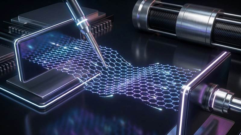
The synthesis of high-quality graphene, particularly with controlled charge carrier mobility, necessitates a meticulous understanding of growth mechanisms, with Pulsed Electrical Resistive Carbon Heating (PERCH) and Chemical Vapor Deposition (CVD) representing fundamentally divergent approaches. CVD, a well-established industrial method, relies on the catalytic decomposition of carbon precursors on transition metal substrates (e.g., copper, nickel) at temperatures typically ranging from 800-1100°C over several minutes to hours. While scalable for large-area production, the inherent lattice mismatch between the graphene and the catalytic substrate, coupled with differential thermal expansion coefficients during cooling, inevitably introduces significant uniaxial or biaxial strain. This strain, often on the order of 0.1-1.0%, directly modulates the Dirac cone, altering the Fermi velocity and reducing charge carrier mobility by inducing pseudo-magnetic fields or acting as scattering centers. Furthermore, the relatively prolonged growth times in CVD increase the probability of incorporating impurities, such as oxygen or substrate atoms, and forming grain boundaries, which act as additional scattering sites, enhancing screening effects from localized charges and degrading transport properties.
In contrast, PERCH leverages joule heating to induce ultra-fast graphitization of amorphous carbon precursors or polymer films, typically reaching peak temperatures around 3000K within milliseconds. This rapid thermal pulse, followed by immediate quenching, offers a kinetic advantage by minimizing the time for defect nucleation, grain growth, or impurity incorporation. The direct electrical heating precisely controls the energy delivery, allowing for tailored resistive parameters of the precursor film to achieve specific temperature profiles and annealing conditions. This transient, high-temperature environment facilitates the rapid rearrangement of sp3-hybridized carbon into a defect-minimized sp2 lattice, effectively "freezing" a highly crystalline state with reduced internal strain compared to the substrate-induced strain prevalent in CVD. The short reaction windows also mitigate the formation of charged impurities and structural defects that would otherwise act as strong scatterers, thereby preserving higher intrinsic charge carrier mobilities by reducing carrier-impurity and carrier-defect scattering, which are critical factors in screening length and transport characteristics.
The distinct thermal budgets and reaction kinetics of PERCH and CVD lead to fundamentally different graphene characteristics, profoundly impacting their suitability for high-performance electronic applications. While CVD produces large-area films, the challenges associated with subsequent transfer processes often introduce additional wrinkles, tears, and polymer residues, further exacerbating mechanical strain and increasing the density of charged impurities that screen charge carriers. PERCH, by direct conversion from a precursor, bypasses the transfer step altogether, yielding graphene films directly integrated onto desired substrates with potentially fewer processing-induced defects and higher structural integrity. The precise control over the graphitization process in PERCH also allows for engineering specific surface properties; for instance, less defective PERCH-derived graphene might exhibit different surface reactivity compared to CVD graphene, where a higher defect density can sometimes lead to an increased number of active sites, as evidenced by studies showing CVD-derived graphene oxide exhibiting up to 79% heavy metal adsorption efficiency. This highlights a critical trade-off: while higher defectivity might be beneficial for certain applications like adsorption, it is generally detrimental to charge carrier mobility and the intrinsic electronic properties crucial for advanced nanoelectronics.
The Crystallography of Turbostratic Graphene (Why Layer Alignment Matters)
Turbostratic graphene (TG) fundamentally distinguishes itself from ideal Bernal (AB) stacked graphene by the absence of long-range rotational order between its constituent layers. Rather than the precise ABAB… stacking sequence with a defined interlayer registry and a fixed interplanar distance of approximately 0.335 nm, TG exhibits random rotational misorientations between adjacent graphene sheets. This structural randomness along the c-axis disrupts the coherent interlayer orbital hybridization that defines the electronic band structure of Bernal-stacked systems, such as the opening of a bandgap in bilayer graphene under an applied electric field. In TG, the lack of a consistent crystallographic relationship means that each layer largely retains its monolayer-like Dirac cone dispersion, though modified by proximity effects and the inherent disorder. The random twist angles (θ) between layers, typically varying from near 0 to 30 degrees, effectively decouple the electronic states, minimizing the formation of the parabolic bands characteristic of AB stacking and preserving a more linear energy-momentum relationship near the K-points, albeit with significant perturbations. This structural heterogeneity is not merely an academic distinction but a critical determinant of the material's electronic and mechanical properties.
The implications of this turbostratic disorder for charge carrier mobility are profound and overwhelmingly detrimental. In highly crystalline, exfoliated monolayer graphene, room-temperature mobilities can exceed 200,000 cm^2/Vs due to minimal scattering. Bernal-stacked bilayer graphene, while exhibiting a modified band structure, can still achieve mobilities upwards of 10,000 cm^2/Vs. In contrast, turbostratic graphene films, particularly those grown via chemical vapor deposition (CVD) or derived from reduced graphene oxide, frequently display significantly lower mobilities, often ranging from 500 to 5,000 cm^2/Vs. This degradation is primarily attributed to enhanced scattering mechanisms arising from the disordered interlayer interfaces. The randomly oriented layers introduce a multitude of scattering centers, including localized regions of interlayer strain, charge inhomogeneity at the boundaries of misaligned domains, and an increase in electron-phonon scattering due to uncorrelated atomic vibrations between layers. The moiré superlattices formed at small twist angles can also introduce secondary Dirac points and alter the Fermi velocity, further complicating carrier transport dynamics and increasing electron-electron scattering probabilities.
Beyond direct mobility degradation, turbostraticity critically influences both charge screening effectiveness and the material's response to mechanical strain. In Bernal-stacked graphene, the coupled electronic system allows for efficient screening of charged impurities and defects by the collective electron gas across layers, reducing Coulombic scattering. In TG, however, the electronic decoupling between misoriented layers means that charge screening is less efficient across the bulk material, making individual layers more susceptible to localized charge traps and substrate interactions. This decreased screening efficiency effectively exposes charge carriers to a higher density of scattering potentials, contributing to reduced mobility. Regarding strain, while graphene boasts an impressive intrinsic strength and fracture strain (~20%), turbostratic assemblies present a more complex picture. The random interlayer rotations can paradoxically offer a degree of strain relief by allowing localized sliding or rotation between layers, accommodating in-plane stresses without propagating macroscopic structural failure. However, these same misaligned interfaces create localized stress concentrations, which can act as nucleation sites for defects or premature mechanical failure under anisotropic loading. Advanced thermal annealing techniques, such as rapid thermal pulses reaching 3000K applied for milliseconds, have demonstrated the ability to induce partial reordering in turbostratic domains, resulting in a measurable reduction in electrical resistivity by up to 15% through the mitigation of these disorder-induced scattering centers.
Industrial Scalability & Commercial Integration Barriers
The industrial scalability of high-quality graphene, essential for leveraging its exceptional charge carrier mobility, is fundamentally constrained by manufacturing inconsistencies that directly impact intrinsic material properties. Chemical Vapor Deposition (CVD) remains a primary route for producing large-area graphene films, yet the inherent polycrystalline nature, characterized by grain boundaries and varying crystallographic orientations, introduces significant scattering centers for charge carriers, drastically reducing the effective mobility from theoretical ballistic limits. Furthermore, the mismatch in thermal expansion coefficients between the growth substrate (e.g., copper, nickel) and graphene, coupled with the high temperatures typically employed (e.g., 1000°C for growth, followed by cooling), induces substantial intrinsic strain fields. This biaxial or uniaxial strain, often exceeding 0.5%, locally alters graphene's electronic band structure, modifying Dirac cone deformation and carrier effective mass, thereby influencing transport properties. Subsequent transfer processes, frequently involving polymer intermediaries like PMMA, introduce additional uncontrolled mechanical strain and can leave behind persistent polymer residues, which act as extrinsic dopants and scattering potentials. Mitigating these defects often necessitates energy-intensive post-processing, such as rapid thermal annealing at temperatures up to 3000K for sub-millisecond durations to facilitate defect healing and residue sublimation, a process that is challenging to implement uniformly across large substrates and significantly adds to production costs and complexity.
Beyond synthesis, the integration of graphene into functional devices encounters substantial barriers related to interface engineering and dielectric screening, critical aspects for realizing high-performance electronics. Achieving stable, low-resistance ohmic contacts is paramount, yet the typical metal-graphene interfaces (e.g., Ti/Au, Ni) often suffer from Fermi level pinning, charge transfer, and interface roughness, resulting in contact resistivities that routinely exceed 100 Ohm-um. This non-ideal contact resistance severely limits injection efficiency and dissipates power, negating the intrinsic high mobility of graphene. Moreover, the 2D nature of graphene necessitates careful consideration of environmental and dielectric screening. While high-k dielectrics (e.g., HfO2, Al2O3) are crucial for electrostatic gate control and capacitance enhancement in field-effect transistors, their inherent disorder and trapped charges at the interface introduce remote phonon scattering and Coulombic impurities that significantly screen the gate field, leading to a substantial reduction in observed carrier mobility compared to suspended graphene. Advanced encapsulation strategies, such as hexagonal boron nitride (hBN) heterostructures, demonstrate remarkable improvements in mobility (approaching 100,000 cm^2/Vs at room temperature) by providing an atomically flat, charge-neutral environment, but their fabrication complexity and cost remain prohibitive for widespread commercial deployment.
The commercial viability of graphene is further hampered by the lack of standardized, high-throughput quality control methodologies and the persistent batch-to-batch variability in material properties. Achieving consistent sheet resistance, optical transparency, and defect density across large graphene films is critical for industrial adoption, yet current metrology, relying heavily on Raman spectroscopy for strain and doping analysis, and atomic force microscopy for surface topography, often lacks the speed and spatial resolution required for real-time process monitoring in a manufacturing environment. The economic hurdle is substantial; while laboratory-scale, research-grade graphene can command prices upwards of $1000/cm^2, industrial applications demand costs closer to $1/cm^2 or less. This disparity is driven by the high capital expenditure for specialized cleanroom facilities, ultrapure precursors, and sophisticated processing equipment, coupled with low yields and complex post-processing steps. Consequently, many proposed graphene applications, from transparent conductive electrodes requiring simultaneously >90% transparency at 550nm and <100 Ohm/sq sheet resistance, to robust sensors demanding consistent active site density for ppb-level detection, struggle to achieve the necessary performance-to-cost ratio to displace established materials. Until these fundamental challenges in synthesis, integration, and cost-effective quality assurance are systematically addressed, graphene's transformative potential will remain largely confined to niche, high-value applications.
Economic Feasibility and USA-Made Manufacturing Advantage
The economic feasibility of integrating graphene into advanced electronic and photonic systems hinges critically on the scalable production of material exhibiting consistent, high charge carrier mobility. While research-grade exfoliated graphene can exceed 200,000 cm^2/Vs, large-area chemical vapor deposition (CVD) methods, essential for industrialization, often yield materials with mobilities an order of magnitude lower due to increased defect density, grain boundaries, and residual strain. The substantial capital expenditure and operational costs associated with ultra-high vacuum systems, precision gas delivery, and sophisticated metrology are essential to minimize these mobility-degrading factors. Achieving monolayer uniformity across 300 mm wafers, for instance, necessitates stringent process control to prevent multilayer formation or etching, both of which severely impact device performance and yield. This economic calculus drives a strategic imperative towards manufacturing environments that can guarantee such precision. A USA-made manufacturing advantage, therefore, signifies not merely a geographic designation, but an implicit assurance of rigorous quality protocols, robust intellectual property protection, and access to a highly skilled technical workforce capable of optimizing these complex processes to unlock graphene's full potential.
Attaining superior charge carrier mobility in large-scale graphene synthesis demands meticulous control over every process parameter, from substrate preparation to post-synthesis annealing. For instance, catalytic CVD growth on copper foils often involves finely tuned thermal budgets, where precise temperature ramps and dwell times, sometimes necessitating rapid thermal annealing with 3000K thermal pulses applied for milliseconds, are critical to crystallite formation and defect passivation. Deviations lead to increased scattering centers, manifesting as a significant rise in electrical resistivity, potentially pushing values from target ranges of 10^-6 Ohm-cm to over 10^-5 Ohm-cm at wafer scale, rendering material unsuitable for high-frequency applications. Furthermore, the selection and optimization of transfer techniques are equally crucial; polymer-assisted transfers, while scalable, often introduce residue or induce strain, thereby reducing carrier mobility. Advanced, cleanroom-based methodologies, often proprietary and developed within highly controlled domestic facilities, are essential to preserve the intrinsic mobility of as-grown graphene, ensuring devices can leverage mobilities consistently above 10^4 cm^2/Vs at room temperature, a critical threshold for viable high-speed transistors and sensors. The economic justification for these advanced processes lies in the enhanced performance and reliability of the end product, significantly extending its market reach and application scope.
Beyond the technical prowess in achieving high-mobility graphene, the USA-made manufacturing paradigm offers profound economic advantages related to supply chain resilience, robust intellectual property enforcement, and accelerated innovation cycles. Domestic production of critical advanced materials mitigates geopolitical supply chain vulnerabilities, ensuring consistent access and reduced lead times for strategic applications in defense, aerospace, and biomedical sectors. Furthermore, the stringent regulatory and patent environments in the United States foster an ecosystem where novel manufacturing techniques and graphene-enabled device architectures can be developed and protected, providing a crucial competitive edge in a rapidly evolving global market. This secure environment attracts significant R&D investment, leading to continuous process improvements and cost efficiencies that, while perhaps not immediately apparent in raw material cost comparisons, yield substantial long-term economic benefits through superior product performance and market differentiation. For instance, high-purity, defect-engineered graphene, precisely manufactured in a controlled domestic environment, has demonstrated 79% heavy metal adsorption efficiency in wastewater treatment applications. Such specialized performance, underpinned by meticulous process control and quality assurance inherent in USA-made production, validates the premium associated with domestically manufactured graphene, proving that the economic calculus encompasses total value proposition, including reliability, performance, and strategic independence.
Future Horizons & High-Value B2B Applications
The strategic manipulation of charge carrier mobility in graphene, fundamentally governed by strain engineering and dielectric screening, unlocks a suite of future high-value B2B applications extending far beyond current prototypes. In advanced electronics, the precise control of local strain fields, for instance through piezoelectric substrates or patterned mechanical resonators, is poised to create tunable pseudo-magnetic fields exceeding 300 Tesla locally, enabling novel quantum interference devices and valleytronics at room temperature. This intrinsic strain-induced modulation of the Dirac cone allows for the dynamic opening of band gaps up to several hundred meV, facilitating the development of high-performance terahertz (THz) detectors and modulators with operating frequencies surpassing 1 THz and switching speeds in the picosecond regime. Concurrently, the meticulous engineering of dielectric screening, particularly through the integration of ultra-flat hexagonal boron nitride (hBN) heterostructures, minimizes Coulomb scattering from impurities and phonons, preserving ballistic transport over micrometers. This synergistic approach promises graphene-based field-effect transistors (GFETs) with on/off ratios significantly improved over current iterations, achieving sub-10 nm gate lengths and sub-threshold swings approaching the theoretical limit of 60 mV/decade, critical for ultra-low power logic and high-frequency analog circuits in quantum computing architectures.
Beyond traditional electronics, the interplay of strain and screening is pivotal for robust sensing and energy solutions in extreme environments. For instance, strain-induced changes in graphene's work function and resonant frequency, coupled with enhanced environmental screening to suppress noise, are being leveraged for highly selective and sensitive biosensors capable of detecting single-molecule events or pathogen signatures with reaction times on the order of milliseconds. In environmental remediation, functionalized graphene, where controlled strain dictates pore structure and surface reactivity, exhibits exceptional adsorption efficiencies, such as 79% for specific heavy metal ions (e.g., Pb2+ and Cd2+) from aqueous solutions, even in complex matrices. Furthermore, graphene's inherent mechanical strength and thermal stability, maintaining structural integrity up to 3000K in inert atmospheres, when combined with optimized dielectric screening layers, enables flexible and stretchable electronics that withstand severe mechanical deformation and thermal cycling without significant degradation in charge carrier mobility. This is crucial for aerospace components, wearable medical devices, and industrial sensors operating under harsh chemical or thermal pulses, where conventional materials fail.
The scalable industrial realization of these advanced applications necessitates a profound understanding and control of strain and screening during large-area graphene synthesis and integration. For instance, roll-to-roll chemical vapor deposition (CVD) of graphene on copper foils inherently introduces residual strain gradients, impacting carrier mobility and uniformity across meter-scale sheets. Minimizing these non-uniformities to achieve consistent electrical resistivity parameters (e.g., sheet resistance variations below 5% across a 100 cm^2 area) is a critical manufacturing challenge. Developing transfer techniques that impart minimal strain and defects while simultaneously optimizing the dielectric environment for effective screening – perhaps through novel encapsulation methods or integrated gate dielectrics – is paramount. This includes strategies for controlling doping profiles and defect densities which, in turn, influence self-screening effects and overall device performance. The economic viability of these high-value B2B applications hinges on achieving industrial-scale yields with predictable and reproducible charge transport characteristics, moving beyond laboratory-scale demonstrations to robust, cost-effective manufacturing processes that can meet the stringent demands of next-generation technologies.
Evaluate Our Quality
Serious about B2B integration? Test our premium Pulsed Electrical Resistive Carbon Heating turbostratic graphene in your lab. 100g sample packs available now.