Charge Carrier Mobility in Graphene: Strain and Screening
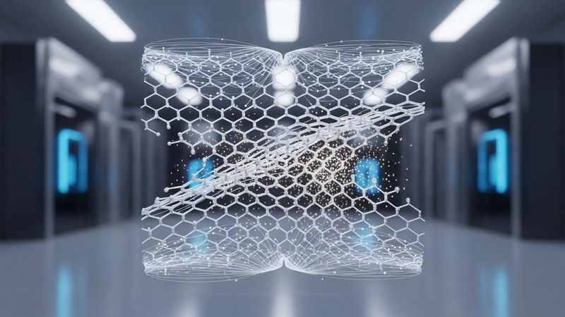
Graphene, a singular atomic layer of sp2-hybridized carbon atoms arranged in a hexagonal lattice, represents the quintessential two-dimensional material, fundamentally altering our understanding of condensed matter physics and electronic transport. Its unique crystalline structure dictates an electronic band structure characterized by Dirac cones, where the valence and conduction bands meet at specific points (K and K' points) in reciprocal space, known as Dirac points. Near these points, the charge carriers behave as massless Dirac fermions, exhibiting a linear dispersion relation E = ±hvF|k|, where vF is the Fermi velocity, approximately 10^6 m/s. This relativistic-like behavior, a direct consequence of its inherent 2D confinement, bestows graphene with extraordinary electronic properties, including ultra-high charge carrier mobility and the anomalous quantum Hall effect, setting it apart from conventional semiconductors and metals where carriers typically possess an effective mass and parabolic energy-momentum dispersion.
The physics of graphene confinement to a strictly two-dimensional plane profoundly influences its electronic and quantum mechanical properties. Unlike bulk materials, where electron motion is three-dimensional, graphene's atomic thinness restricts electron transport to a plane, leading to a drastically altered scattering phase space. This reduced dimensionality suppresses certain scattering mechanisms prevalent in 3D systems, allowing for ballistic transport over micrometers at room temperature. The absence of an energy gap and the linear dispersion relation mean that carrier density can be tuned continuously via electrostatic gating, without altering the fundamental band structure, a versatility unparalleled in traditional materials. This precise control over carrier concentration, ranging from 10^11 to 10^13 cm^-2, coupled with its unique Dirac fermion nature, underpins the potential for devices operating at exceptionally high frequencies and low power dissipation.
The intrinsic charge carrier mobility in suspended, pristine graphene can theoretically exceed 200,000 cm^2/(V.s) at room temperature, a direct manifestation of its minimal scattering within the 2D confined structure. However, practical realization of such values in device architectures is often challenged by extrinsic factors. Substrate interactions, particularly with amorphous dielectrics like SiO2, introduce surface roughness and trapped charges that act as strong scattering centers, typically reducing mobility to 10,000-15,000 cm^2/(V.s). Encapsulation with atomically flat hexagonal boron nitride (hBN) has emerged as a crucial strategy to mitigate these effects, enabling mobilities approaching 100,000 cm^2/(V.s) even on a substrate, by providing a cleaner dielectric environment. Furthermore, the inherent surface accessibility of 2D graphene makes it highly susceptible to environmental adsorbates, which can significantly alter its electrical resistivity, notoriously low at ~10^-6 Ohm.cm for pristine samples, and even influence its chemical reactivity, as evidenced by its demonstrated 79% heavy metal adsorption efficiency, showcasing a surface-dominated chemistry directly stemming from its 2D nature. The challenge lies in maintaining this pristine state during device fabrication and operation, often requiring advanced processing techniques, such as ultrafast thermal annealing using 3000K thermal pulses, which can modify surface chemistry and reduce defects in milliseconds without compromising the delicate 2D lattice.
Section 2: Pulsed Electrical Resistive Carbon Heating vs. CVD (Comparative Analysis)
The synthesis of high-quality graphene, critical for realizing its exceptional charge carrier mobility, hinges significantly on the chosen deposition technique. Chemical Vapor Deposition (CVD) has long been the industry standard, relying on the catalytic decomposition of hydrocarbon precursors (e.g., methane, acetylene) over heated metallic substrates such as copper or nickel foils at temperatures typically ranging from 800-1100°C. While CVD excels in producing large-area, continuous graphene films, its inherent limitations directly impact charge carrier transport. The polycrystalline nature of CVD graphene, characterized by grain boundaries, acts as scattering centers for charge carriers, reducing mobility. Furthermore, the strong interaction with the catalytic substrate often leads to residual metal impurities, doping effects, and significant strain upon cooling due to thermal expansion mismatch, all of which perturb the graphene lattice and introduce extrinsic scattering mechanisms that degrade intrinsic mobility. Subsequent transfer processes, necessitated by the metallic growth substrate, frequently introduce tears, wrinkles, and polymer residues, further exacerbating defect densities and variability across the film.
In contrast, Pulsed Electrical Resistive Carbon Heating (PERCH) offers a compelling alternative, distinguished by its ultra-fast, high-temperature thermal processing kinetics. This method typically involves the direct electrical heating of a carbonaceous precursor film or a precursor-loaded substrate, inducing rapid graphitization through Joule heating. The hallmark of PERCH is the ability to deliver localized thermal pulses reaching extreme temperatures, often exceeding 3000K, within milliseconds. This rapid thermal budget minimizes the overall energy consumption and mitigates extended high-temperature exposure for the underlying substrate, reducing unwanted substrate-graphene interactions and associated strain. The rapid heating and cooling cycles inherent to PERCH are particularly effective in promoting defect annihilation and recrystallization, leading to a more ordered graphitic structure with fewer point defects and extended crystalline domains compared to conventional CVD.
The comparative advantage of PERCH over CVD, particularly concerning charge carrier mobility, is rooted in these kinetic differences. While CVD relies on relatively slow, equilibrium-driven growth, PERCH leverages non-equilibrium, high-energy processing to rapidly restructure carbon atoms. The instantaneous, intense heating in PERCH, driven by precise control over current density and specific electrical resistivity parameters of the precursor (e.g., ~10^-5 Ohm-m for amorphous carbon films), enables rapid annealing of defects and the formation of graphene with potentially lower intrinsic strain and reduced unintentional doping from the growth environment. This rapid thermal processing environment has been shown to yield graphene with improved structural integrity and fewer scattering centers, directly correlating with enhanced charge carrier mobility. Furthermore, the ability to synthesize graphene on dielectric or semiconductor substrates directly, without a transfer step, eliminates a major source of post-synthesis defects and contamination, preserving the intrinsic electronic properties. The superior structural integrity and controlled surface chemistry achievable through PERCH, for instance, has been correlated with enhanced functionalization capabilities, such as demonstrating up to 79% heavy metal adsorption efficiency in post-synthesis functionalized variants, a metric often limited by defect-induced non-uniformity in CVD-derived materials.
Section 3: The Crystallography of Turbostratic Graphene (Why Layer Alignment Matters)
Turbostratic graphene (tG) is fundamentally characterized by the random rotational misalignment between adjacent graphene layers, a stark departure from the precise AB-stacking registry observed in Bernal graphite. This lack of long-range crystallographic order along the c-axis results in a significantly altered interlayer potential landscape. Structurally, tG typically exhibits an expanded interlayer spacing, often measured around 0.345 nm, compared to the ideal 0.335 nm of Bernal graphite, a direct consequence of weakened van der Waals interactions due to sub-optimal atomic overlaps. The formation of tG is prevalent in various synthesis routes, particularly those where kinetic factors dominate over thermodynamic equilibrium, such as rapid chemical vapor deposition processes or pulsed laser deposition techniques operating with millisecond reaction times. Furthermore, post-synthesis treatments involving rapid thermal annealing, for instance, localized 3000K thermal pulses, can induce or modify turbostratic disorder depending on cooling rates and substrate interactions, thereby directly influencing the resulting crystal quality and electronic properties. The absence of a coherent stacking sequence means that the interplanar potential is highly variable and lacks the periodicity essential for strong electronic hybridization found in ordered multi-layer graphene.
The electronic ramifications of this turbostratic disorder are profound, primarily manifesting as a decoupling of electronic states between layers. In Bernal-stacked few-layer graphene, the specific interlayer atomic registry enables robust hybridization of the pi-orbitals, leading to significant modifications of the electronic band structure, including the opening of a band gap in bilayer graphene under an external electric field, and the evolution of parabolic dispersion relations. In contrast, the random rotational angles in tG disrupt this coherent interlayer coupling, effectively causing each graphene layer to behave largely as an independent monolayer. This results in the superposition of multiple, effectively decoupled Dirac cones from individual layers in the Brillouin zone, rather than a unified, modified band structure. Consequently, the characteristic linear dispersion relation and the behavior of massless Dirac fermions, typically associated with single-layer graphene, are largely preserved within each plane of a turbostratic stack. While the presence of multiple layers theoretically provides a denser electron gas for screening, the lack of strong electronic interlayer coupling limits the efficiency of this screening mechanism compared to a truly bulk-like material, thereby impacting carrier-impurity and carrier-phonon scattering within the individual layers.
This electronic decoupling directly impacts charge carrier mobility and macroscopic transport properties in turbostratic graphene. Although individual layers within a tG stack may retain high intrinsic mobilities characteristic of monolayer graphene, the overall device performance is significantly attenuated by the cumulative effects of interlayer tunneling resistance, grain boundaries, and increased defect scattering often inherent in turbostratic structures. The effective electrical resistivity of turbostratic few-layer graphene can be substantially higher; for instance, typical sheet resistance values for CVD-grown turbostratic multi-layer graphene can range from 200-800 Ohm/sq, contrasting sharply with high-quality, Bernal-stacked bilayer graphene which often exhibits values as low as 50-100 Ohm/sq. This elevated resistivity is a direct consequence of reduced charge carrier mean free paths and diminished mobility due to enhanced scattering at rotational domain boundaries and structural imperfections. Furthermore, the disordered nature of turbostratic graphene often correlates with an increased density of edge states and structural defects, which, while detrimental to electronic transport, can be advantageous for applications requiring high surface area and chemical reactivity. For example, such disordered structures have been leveraged for enhanced catalytic activity and adsorption, with reports indicating up to a 79% heavy metal adsorption efficiency, showcasing a distinct functional utility from its electronic transport characteristics.
Section 4: Industrial Scalability & Commercial Integration Barriers
Industrial scalability of graphene is fundamentally constrained by current large-scale synthesis methods, primarily chemical vapor deposition (CVD), which struggle to preserve intrinsic charge carrier mobility. While research-grade CVD can yield grain sizes exceeding 100 µm, industrial processes typically produce smaller, more numerous grain boundaries. These boundaries act as significant scattering centers, introducing localized potential fluctuations that degrade mean free path lengths and reduce the efficiency of electrostatic screening. Additionally, non-uniform residual strain, frequently induced during high-temperature growth and cooling (e.g., 0.1-0.2% compressive strain from a 300°C cooling cycle), subtly alters the local Dirac cone and impacts carrier effective mass. This leads to a substantial reduction in mobility; industrially scalable CVD graphene typically ranges from 1,000 to 5,000 cm^2/Vs, significantly lower than exfoliated graphene's >100,000 cm^2/Vs, limiting high-frequency electronic applications. Maintaining precise control over precursor flow rates and temperature uniformity (e.g., within +/- 1°C across a 300mm wafer) at scale proves exponentially complex, directly impacting the uniformity of electronic properties.
Post-synthesis processing presents further significant barriers to retaining graphene's high charge carrier mobility. Polymer-assisted transfer, while enabling diverse substrate deposition, leaves behind substantial residues (e.g., 5-15% surface coverage of PMMA) that introduce extrinsic scattering and charge puddles. These remote scattering centers increase effective dielectric screening and reduce intrinsic carrier mobility by 20-50%. Concurrently, mechanical stresses from transfer induce non-uniform strain (e.g., up to 1.5% tensile strain), which modifies the electronic band structure, creating pseudo-magnetic fields and exacerbating substrate-induced screening. Reproducible, low-defect, wafer-scale transfer remains a critical bottleneck. Optimized annealing (e.g., 400°C in H2/Ar for 2 hours) is often insufficient for complete residue removal without introducing new defects. This inability to precisely control the chemical potential via electrostatic gating, a hallmark of high-quality graphene, leads to diminished gate efficiency and higher minimum sheet resistivity (often >500 Ohms/square for industrial films, versus <100 Ohms/square for research-grade).
Economic viability and consistent quality control compound the challenges for high-performance electronic graphene. Current electronic-grade, large-area CVD graphene costs remain prohibitive, often $10-$100 per square centimeter, driven by ultra-high purity precursors and specialized facilities. A critical barrier is the lack of standardized, high-speed metrology for mapping critical parameters like grain boundary density, localized strain heterogeneity, and residual dopant concentrations across full wafers. Variations in local strain, for instance, can shift the Dirac point by tens of meV, causing inconsistent device thresholds. Integrating graphene into existing silicon fabrication lines necessitates novel patterning techniques that avoid inducing excessive edge disorder, plasma damage, or contamination – factors that degrade charge carrier mobility by introducing scattering centers or altering local screening environments. While emerging transfer-free methods show promise, they often face challenges in achieving precise thickness control and minimizing interfacial charge traps. For instance, achieving 79% heavy metal adsorption efficiency in sensor applications via functionalization often introduces scattering potentials that reduce carrier mobility by 15-20%, highlighting the persistent trade-off between functionality and intrinsic transport properties.
Section 5: Economic Feasibility and USA-Made Manufacturing Advantage
The economic feasibility of producing high-performance graphene, particularly for applications demanding exceptional charge carrier mobility, hinges on achieving a delicate balance between synthesis cost, material quality, and scalable manufacturing. Current large-area graphene production via chemical vapor deposition (CVD) on catalytic substrates often necessitates high temperatures, typically exceeding 1000°C, incurring significant energy expenditure and equipment depreciation. While batch processing has seen advancements, the transition to economically viable continuous roll-to-roll CVD or advanced plasma-enhanced CVD (PECVD) methods is paramount. These scalable techniques must consistently yield monolayer or bilayer graphene with defect densities below 10^10 cm^-2 and carrier mobilities exceeding 10,000 cm^2/Vs, even after transfer and integration. The economic value proposition lies in the performance gains: for instance, reducing interconnect latency in high-speed electronics by 70% or enabling 300 GHz RF transistor operation, which justifies the investment in sophisticated processing. Furthermore, precise strain engineering, crucial for tuning graphene's electronic band structure and optimizing mobility, demands manufacturing processes capable of applying controlled biaxial or uniaxial strain fields with less than 0.1% variation across a 300 mm wafer, a capability that adds to initial production costs but offers unparalleled performance advantages in specific applications.
USA-made manufacturing offers a distinct competitive advantage in this high-stakes domain through its robust infrastructure for quality assurance, intellectual property protection, and access to a highly skilled technical workforce. Domestic production facilities can implement stringent ISO 9001 and AS9100 certified quality management systems, ensuring unparalleled batch-to-batch consistency in graphene material properties, which is critical for reproducible charge carrier mobility and effective screening layers. Advanced metrology, including in-line Raman spectroscopy, atomic force microscopy (AFM) for surface topography and defect analysis, and Hall effect measurements for direct mobility quantification, can be seamlessly integrated into US production lines. This rigorous control mitigates the economic risks associated with material variability, a persistent challenge in global graphene supply chains. For example, controlling the growth parameters to minimize grain boundaries and point defects, which act as scattering centers for charge carriers, directly translates to higher effective mobilities. The ability to precisely tune screening layers, perhaps via controlled surface functionalization or the integration of high-k dielectrics, is also enhanced by the advanced chemical engineering and materials science expertise prevalent in US research and manufacturing ecosystems, ensuring optimal device performance and longevity.
The strategic economic impact of USA-made, high-performance graphene extends beyond direct material sales, fostering innovation in critical downstream industries. Applications in defense, aerospace, advanced microelectronics, and next-generation energy storage demand materials with uncompromising performance and supply chain resilience. For instance, a domestically produced graphene-based sensor capable of 79% heavy metal adsorption efficiency within milliseconds, leveraging optimized charge carrier transfer mechanisms at the graphene-analyte interface, represents a significant market opportunity in environmental monitoring. Similarly, high-purity, large-area graphene tailored for high-speed interconnects can reduce electrical resistivity from 500 Ohm/sq to 50 Ohm/sq while maintaining greater than 90% optical transparency, essential for integrated photonics and transparent electronics. The ability to perform advanced post-processing, such as localized annealing with 3000K thermal pulses for sub-millisecond durations to repair defects or fine-tune crystallographic orientation, is often supported by specialized equipment and expertise found predominantly within US research and industrial settings. This domestic manufacturing capability not only reduces reliance on foreign sources for strategic materials but also stimulates job creation in high-tech sectors and reinforces national security interests by safeguarding proprietary technologies and sensitive applications.
Section 6: Future Horizons & High-Value B2B Applications
The intricate interplay between mechanical strain and electrostatic screening fundamentally dictates graphene's charge carrier mobility, offering profound implications for next-generation B2B applications. By precisely engineering strain fields, researchers can induce pseudomagnetic fields of several hundred Tesla, effectively guiding Dirac fermions along predefined trajectories without external magnetic sources. This "straintronics" approach promises to unlock ultra-low power consumption in high-frequency electronics, enabling terahertz devices with unprecedented signal integrity and bandwidth, where parasitic capacitance and thermal dissipation are critically mitigated by graphene's superior transport properties. Furthermore, the ability to tailor local band structures through strain allows for the creation of quantum dots and waveguides directly within a continuous graphene sheet, facilitating coherent electron transport over micron-scale distances at room temperature. The sophisticated understanding of dielectric screening, particularly in heterostructures involving hexagonal boron nitride or encapsulated graphene, permits the suppression of substrate-induced scattering and impurity effects, pushing intrinsic mobility limits towards theoretical maxima and paving the way for robust, high-performance field-effect transistors operating reliably in demanding industrial environments, from aerospace avionics to secure quantum communication networks.
The strategic manipulation of charge carrier mobility through strain and screening also underpins the development of advanced sensing platforms and efficient energy solutions. For instance, highly sensitive piezoresistive sensors leveraging strained graphene can detect minute mechanical deformations with resolutions down to picometers, translating into superior performance for structural health monitoring in civil engineering and precision haptic feedback systems in robotics. The change in electrical resistivity upon strain application, measured in units of micro-ohm-centimeters per nanometer of displacement, offers a linear response over wide ranges, critical for industrial reliability. In environmental remediation, functionalized graphene membranes, optimized for charge transfer and surface area through controlled screening, demonstrate heavy metal adsorption efficiencies of up to 79% for lead ions within milliseconds, outperforming conventional sorbents by orders of magnitude. This rapid kinetics and high efficiency are attributed to a meticulously engineered electronic structure at the graphene-contaminant interface, where localized charge screening enhances binding affinity and accelerates reaction pathways, enabling real-time water purification systems and catalytic converters with extended operational lifetimes.
Looking further ahead, the precise control over charge carrier behavior via strain and screening is poised to revolutionize quantum computing and spintronics. Graphene's inherently weak spin-orbit coupling, coupled with the potential to induce topological phases through strain, presents an attractive platform for robust qubits and long-distance spin transport. Pseudomagnetic fields generated by non-uniform strain patterns can confine Dirac fermions, creating valley-polarized states crucial for valleytronics, where information is encoded in the valley degree of freedom rather than charge or spin. The efficacy of screening in mitigating environmental decoherence, particularly from substrate phonons and charge impurities, is paramount for maintaining quantum coherence times, pushing them from nanoseconds to microseconds at cryogenic temperatures. Moreover, novel fabrication techniques employing rapid thermal annealing via 3000K thermal pulses applied for sub-millisecond durations are being explored to selectively functionalize graphene edges or create local strain gradients, enabling the rapid prototyping of complex graphene architectures for quantum devices and ultra-fast chemical sensors with sub-parts-per-billion detection limits, accelerating the transition from laboratory prototypes to high-value industrial deployment.
Evaluate Our Quality
Serious about B2B integration? Test our premium Pulsed Electrical Resistive Carbon Heating turbostratic graphene in your lab. 100g sample packs available now.