Unlocking Graphene's Potential: B & N Doping for Electronics
Graphene, the celebrated purely two-dimensional crystal of carbon atoms, has captivated the scientific and industrial world with its extraordinary properties. Discovered in 2004, this honeycomb-like structure exhibits remarkable electronic and physical characteristics, earning it accolades and sparking visions of a new era in technology. Its atomic thinness, exceptional strength, and unparalleled electron mobility make it a frontrunner for replacing conventional materials in countless applications. However, for all its promise, graphene possesses a fundamental characteristic that has, until recently, limited its widespread adoption in digital electronics: its zero bandgap. This inherent lack of a bandgap means pristine graphene behaves more like a conductor than a semiconductor, hindering its direct use in transistors, which require precise control over electron flow and the ability to switch between distinct "on" and "off" states. To truly unlock graphene's vast potential in high-performance electronics, scientists have embarked on an intensive quest to engineer this intrinsic electronic property, with boron and nitrogen doping emerging as a profoundly promising solution.
The Zero Bandgap Conundrum: Why Pristine Graphene Isn't a Semiconductor
The concept of a bandgap is central to understanding how materials behave electronically. In semiconductors, a bandgap is an energy range where no electron states can exist, separating the lower-energy valence band (where electrons reside at rest) from the higher-energy conduction band (where electrons can move freely and conduct electricity). For a device like a transistor to function as an effective switch, it must be able to prevent electron flow (the "off" state) and allow it (the "on" state) with minimal energy input. This control is facilitated by the bandgap, which acts as a barrier that electrons must overcome to jump from the valence to the conduction band.
Pristine graphene, however, possesses a zero bandgap, meaning its valence and conduction bands meet at a single point, known as the Dirac point, with no energy separation. This unique electronic structure grants graphene its exceptional electron mobility, allowing electrons to move through the material at relativistic speeds without scattering. While this is ideal for conductive applications such as interconnects or transparent electrodes, it presents a significant hurdle for semiconductor applications. Without a bandgap, graphene cannot be effectively turned "off" because electrons can always flow, preventing the creation of a clear current modulation required for digital logic and memory. This fundamental characteristic has driven researchers to explore various strategies to open and tune a bandgap in graphene, transforming it into a viable semiconductor for advanced electronics.
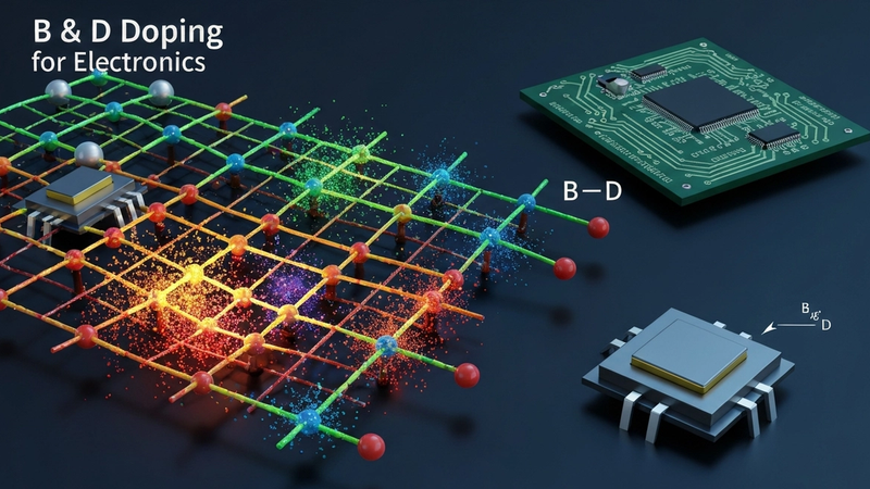
The Promise of Doping: Engineering Graphene's Electronic Properties
The strategic modification of a material's intrinsic electronic properties is a cornerstone of semiconductor technology, commonly achieved through a process known as doping. Doping involves introducing foreign atoms, or dopants, into a crystal lattice to alter the material's electrical conductivity and carrier type. For example, in traditional silicon electronics, phosphorus or arsenic atoms are introduced to create n-type semiconductors by donating extra electrons, while boron atoms are used to create p-type semiconductors by creating "holes" or electron vacancies. This precise control over charge carriers is what enables the complex functionality of modern integrated circuits.
Applying this principle to graphene, doping offers a powerful pathway to overcome its zero bandgap limitation and tailor its electronic behavior. By substituting some of graphene's carbon atoms with atoms from neighboring elements in the periodic table, scientists can subtly perturb its perfect honeycomb lattice and electronic structure. These substitutional dopants introduce localized defects and alter the electron distribution, shifting the Fermi level and potentially opening a bandgap. The choice of dopant atom is critical, as its valence electron configuration dictates whether it will donate electrons (n-type doping) or accept electrons (p-type doping), thereby controlling the type and concentration of charge carriers within the graphene lattice. This ability to engineer graphene's electronic landscape at the atomic level is paramount for its integration into the next generation of electronic devices.
Nitrogen Doping: Creating n-type Graphene and Tailoring the Bandgap
Nitrogen doping stands out as a highly effective method for transforming graphene into an n-type semiconductor and introducing a tunable bandgap. Nitrogen atoms, being in Group 15 of the periodic table, possess five valence electrons, one more than carbon's four. When a nitrogen atom substitutes a carbon atom within the graphene lattice, this extra electron is donated to the surrounding carbon network, effectively increasing the local electron concentration and shifting the Fermi level upwards. This process creates an n-type material, where electrons are the majority charge carriers, analogous to phosphorus-doped silicon.
The presence of nitrogen atoms not only tunes the carrier concentration but also induces structural and electronic perturbations that lead to the opening of a bandgap. Depending on the bonding configuration of nitrogen within the graphene lattice (e.g., pyridinic, pyrrolic, or graphitic N), the bandgap size can be precisely modulated. Graphitic nitrogen, where nitrogen substitutes a carbon atom within the hexagonal ring, is particularly effective at opening a stable bandgap, while also maintaining high electron mobility. Researchers employ various techniques for nitrogen doping, including plasma treatment, chemical vapor deposition (CVD) with nitrogen-containing precursors, and post-synthesis annealing in ammonia atmospheres. These methods allow for fine control over doping concentration and the resulting electronic properties, pushing graphene closer to practical application in advanced electronic circuits.
Boron Doping: Achieving p-type Graphene for Complementary Electronics
Complementary to nitrogen doping, boron doping provides the means to create p-type graphene, a crucial component for building complete electronic circuits. Boron atoms are in Group 13 of the periodic table, possessing only three valence electrons, one fewer than carbon. When a boron atom substitutes a carbon atom in the graphene lattice, it acts as an electron acceptor, effectively creating a "hole" or a missing electron in the carbon network. This process lowers the Fermi level and establishes a p-type semiconductor, where holes are the majority charge carriers, similar to boron-doped silicon.
The introduction of boron atoms also contributes to opening a bandgap in graphene, making it suitable for semiconductor applications. The electron-deficient nature of boron perturbs the local electronic structure, leading to a localized distortion that can separate the valence and conduction bands. Similar to nitrogen doping, the specific bonding configuration of boron within the lattice influences the bandgap magnitude and stability. Techniques such as CVD using boron-containing gases (e.g., diborane) or post-synthesis annealing with boron precursors are employed to achieve controlled boron doping. The ability to precisely tune p-type characteristics in graphene, alongside n-type materials, is foundational for developing complementary metal-oxide-semiconductor (CMOS) logic, which is the bedrock of modern digital electronics.
Synergistic Doping: Fine-Tuning Graphene's Electronic Landscape
While individual boron or nitrogen doping offers significant advancements, the true power of engineering graphene's electronic properties often lies in their synergistic application. Co-doping, or doping graphene with both boron and nitrogen simultaneously, opens up an even broader spectrum of electronic tunability. By carefully controlling the ratio and distribution of B and N atoms within the graphene lattice, researchers can achieve precise control over the bandgap size, the carrier type, and even induce ambipolar behavior, where the material can switch between n-type and p-type conduction depending on the applied gate voltage. This level of fine-tuning is exceptionally difficult to achieve with single-element doping.
The interaction between co-doped B and N atoms can lead to more stable and wider bandgaps compared to single doping, often through the formation of specific B-N bonds or clusters within the carbon matrix. These interactions can create localized charge distributions that strongly influence the overall electronic structure, enhancing device performance. For instance, the creation of B-N bonds can further break the symmetry of the graphene lattice, leading to more pronounced bandgap opening. The challenge, however, lies in achieving homogeneous and controllable co-doping at the atomic level, ensuring that the desired electronic properties are consistently realized across larger areas, which is crucial for scalable manufacturing. Advanced synthesis techniques are continually being refined to address these complexities and unlock the full potential of synergistically doped graphene.
Applications and the Road Ahead: Graphene Electronics Beyond the Lab
The successful engineering of a bandgap in graphene through boron and nitrogen doping has profound implications for its integration into a vast array of electronic applications, moving it from a theoretical marvel to a practical contender. Doped graphene can now form the active channel in field-effect transistors (FETs), enabling the creation of high-speed, low-power logic gates essential for next-generation computing. Its excellent thermal conductivity and mechanical robustness also mean these devices can operate efficiently under demanding conditions, potentially extending battery life and reducing heat generation in electronics.
Beyond digital logic, B and N doped graphene is poised to revolutionize sensor technology. Its high surface-to-volume ratio and tunable electronic properties make it an ideal material for ultra-sensitive gas sensors, biosensors for medical diagnostics, and environmental monitoring devices, capable of detecting minute quantities of target molecules. In energy storage, doped graphene can significantly enhance the performance of supercapacitors and batteries by providing highly conductive and stable electrode materials with increased charge storage capacity. Furthermore, the combination of atomic thinness, flexibility, and transparency makes doped graphene an exceptional candidate for flexible and wearable electronics, smart textiles, and transparent conductive films for advanced displays and solar cells. The journey from lab to market still involves overcoming challenges related to scalable, high-quality production and integration with existing semiconductor infrastructure, but the scientific breakthroughs in B and N doping have undeniably paved the way for a future where graphene-based electronics are ubiquitous.
FAQ
Q1: What is a bandgap and why is it important for electronics?
A1: A bandgap is an energy range within a material where no electron states can exist, separating the valence band (filled with electrons) from the conduction band (where electrons can move freely). For semiconductors, a bandgap is critical because it allows for precise control over electron flow. Devices like transistors rely on the ability to switch between an "on" state (electrons flow across the bandgap) and an "off" state (electron flow is blocked by the bandgap), enabling digital logic and memory functions.
Q2: How does B and N doping physically change graphene?
A2: B and N doping involves replacing some of graphene's carbon atoms with boron or nitrogen atoms within its hexagonal lattice. Nitrogen atoms (5 valence electrons) donate an extra electron to the graphene network, creating an n-type semiconductor. Boron atoms (3 valence electrons) accept an electron from the network, creating a "hole" and forming a p-type semiconductor. These substitutions also perturb the electronic structure, leading to the opening of a tunable bandgap and shifting the Fermi level.
Q3: Are there other ways to create a bandgap in graphene besides B and N doping?
A3: Yes, researchers are exploring several other methods. These include quantum confinement effects (e.g., cutting graphene into narrow nanoribbons), applying external electric fields in bilayer graphene, introducing structural defects, or creating graphene heterostructures with other 2D materials. However, B and N doping offers a particularly robust and controllable method for engineering the bandgap and carrier type directly within the graphene sheet.
Q4: What are the main challenges in manufacturing B and N doped graphene devices?
A4: Key challenges include achieving uniform and precise doping concentrations across large areas, which is essential for consistent device performance and scalability. Controlling the specific bonding configurations of the dopant atoms (e.g., graphitic vs. pyridinic nitrogen) is also difficult but crucial for optimizing bandgap size and stability. Furthermore, integrating doped graphene with conventional semiconductor fabrication processes and ensuring long-term device stability and reliability remain significant hurdles.
Q5: How does doped graphene compare to silicon in future electronics?
A5: Doped graphene offers several advantages over silicon, including ultra-high electron mobility, atomic thinness, flexibility, and transparency, making it ideal for high-speed, flexible, and transparent electronics that silicon cannot easily achieve. While silicon remains the workhorse of current electronics, doped graphene has the potential to complement or even surpass silicon in specific niche applications, especially where speed, power efficiency, and novel form factors are paramount. It represents a pathway to overcome the physical limits of silicon miniaturization.
The ability to precisely control graphene's electronic properties through boron and nitrogen doping marks a pivotal moment in the journey towards realizing its full potential in advanced electronics. By effectively addressing the zero bandgap limitation, researchers have transformed graphene from a fascinating conductor into a versatile semiconductor, opening doors to a new generation of high-performance, energy-efficient, and flexible devices. While significant scientific and engineering challenges remain in scalable manufacturing and integration, the fundamental breakthroughs in B and N doping have firmly established a viable path forward. The future of electronics will undoubtedly be shaped by the continued innovation in engineering this remarkable material, with doped graphene poised to drive advancements across computing, sensing, and energy technologies, ushering in an era of unprecedented technological capability.
Evaluate Our Quality
Serious about B2B integration? Test our premium Pulsed Electrical Resistive Carbon Heating turbostratic graphene in your lab. 100g sample packs available now.