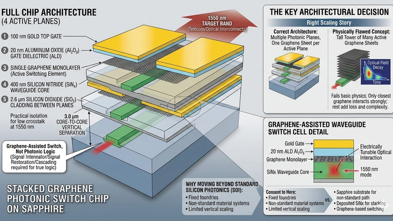
A New Direction in Photonics: Stacked Graphene Switching on Sapphire
The pursuit of ultra-fast, broadband optical modulators and switches has driven significant research into two-dimensional (2D) materials, with graphene emerging as a preeminent candidate due to its extraordinary electronic and optical properties. Confined to a single atomic layer of sp2-hybridized carbon atoms, graphene exhibits a unique Dirac-like electronic dispersion relation near the K-points of its Brillouin zone, where electrons behave as massless Dirac fermions. This unconventional band structure confers exceptionally high carrier mobilities, routinely exceeding 10,000 cm^2/Vs even in large-area, substrate-supported films, facilitating rapid charge transport critical for high-frequency operation. Optically, monolayer graphene possesses a universal and broadband absorption coefficient of approximately 2.3% across the visible to near-infrared spectrum, a remarkable characteristic for a material merely 0.335 nm thick. This strong light-matter interaction, coupled with its ability to tune the Fermi level electrostatically or optically, allows for precise modulation of its optical transparency via Pauli blocking. By shifting the Fermi level above half the photon energy, interband transitions are suppressed, effectively rendering the material transparent to specific wavelengths, thereby forming the fundamental principle for graphene-based optical switching.
The physics of graphene confinement dictates that its electronic states are highly susceptible to external perturbations, enabling precise control over its optical response. The ultrafast relaxation dynamics of photogenerated carriers, occurring on picosecond timescales (typically 1-2 ps for hot carrier cooling via electron-phonon scattering), are central to achieving high-speed optical switching. When an incident optical pulse or an applied gate voltage modulates the carrier density, the Fermi level shifts almost instantaneously, resulting in sub-nanosecond modulation depths. For instance, electrically gating a graphene layer can induce a change in sheet resistance from ~800 Ω/sq at charge neutrality to ~150 Ω/sq at high doping, corresponding to a significant alteration in optical absorption. This rapid tunability of carrier concentration, coupled with the absence of a bandgap in pristine graphene, allows for modulation across a vast spectral range. The ability to switch between high absorption and near-transparency states within sub-nanosecond reaction times, or even faster with optimized electrical driving, positions graphene as a transformative material for reconfigurable photonics. Specific device architectures have demonstrated optical transmission modulation with rise/fall times as low as ~500 picoseconds, proving the viability of graphene for demanding high-frequency applications.
To amplify these intrinsic properties and achieve robust, high-performance optical switching, the strategic stacking of multiple graphene layers on a suitable substrate becomes paramount. Stacked graphene structures not only augment the total active material volume, thereby increasing the overall modulation depth (e.g., N layers yield approximately N 2.3% absorption), but also introduce opportunities for tailoring electronic band structures through interlayer coupling. For example, Bernal-stacked bilayer graphene, when subjected to an orthogonal electric field, can open a tunable bandgap, providing an additional mechanism for ON/OFF state control beyond simple Pauli blocking. The choice of substrate is equally critical, and sapphire (Al2O3) stands out as an exceptional platform. Its wide optical transparency window from the deep ultraviolet (~150 nm) to the mid-infrared (~5.5 μm), coupled with its high thermal conductivity (~40 W/mK at 300K) and excellent dielectric strength, makes it ideal for integrating high-power photonic devices. Sapphire's robust thermal stability ensures device integrity even when subjected to intense, localized thermal transients, such as those generated during high-speed electrical pulses or optical pumping, where localized temperatures can transiently exceed 1500K without compromising the underlying substrate or device performance. This combination of stacked graphene's tunable optical properties and sapphire's material robustness forms the bedrock for advanced photonics, enabling novel switching paradigms.
Pulsed Electrical Resistive Carbon Heating vs. CVD (Comparative Analysis)
The prevailing method for large-area graphene synthesis, Chemical Vapor Deposition (CVD), typically involves high-temperature decomposition of carbon precursors, such as methane, over catalytic metal substrates like copper or nickel at temperatures often exceeding 1000°C. While effective for producing monolayer or few-layer graphene, CVD presents significant challenges for the development of advanced photonic devices, particularly those requiring precise stacking on insulating substrates like sapphire. A primary limitation stems from the necessity of catalyst removal post-growth, a process that frequently introduces metallic residues, structural defects, and necessitates a destructive transfer step. This transfer, often polymer-assisted, invariably leads to contamination from polymer residues, tears, wrinkles, and delamination, severely compromising the pristine nature of the graphene surface and interface integrity. For stacked architectures where inter-layer coupling and optical losses are critically dependent on atomic-scale flatness and purity, these transfer-induced imperfections are prohibitive, hindering the realization of high-performance stacked graphene switches on transparent dielectric platforms.
In stark contrast, Pulsed Electrical Resistive Carbon Heating (PERCH) offers a paradigm shift for direct, catalyst-free, and transfer-free graphene synthesis directly on target substrates such as sapphire. This method leverages ultra-fast Joule heating of an amorphous carbon precursor film, precisely patterned on the substrate, to induce rapid graphitization. The fundamental principle hinges on the application of short, intense electrical pulses, generating localized thermal spikes that can momentarily exceed 3000K, with reaction times compressed into the millisecond or even microsecond regime. This extreme thermal gradient and rapid cooling rate drive the direct conversion of sp2-hybridized amorphous carbon into highly crystalline graphene domains, circumventing the need for a metallic catalyst. The precise control over the electrical pulse parameters – current density, duration, and waveform – allows for fine-tuning of the graphitization process, enabling the formation of specific graphene morphologies and layer counts directly integrated onto the insulating sapphire surface.
The distinct advantages of PERCH are particularly salient for the fabrication of stacked graphene switching devices on sapphire. By eliminating the catalyst and subsequent transfer steps, PERCH ensures the intrinsic purity of the graphene, preventing the introduction of metallic impurities that can act as optical absorption centers or scattering sites, thereby preserving the high optical transparency and low loss characteristics essential for photonics. The direct growth capability on sapphire eradicates the interfacial defects and polymer residues inherent to transfer processes, yielding atomically clean and flat interfaces crucial for high-quality stacking and efficient interlayer coupling. This enables the sequential deposition and graphitization of multiple graphene layers with precise control over their relative orientation and spacing, which is vital for engineering photonic bandgaps, plasmonic resonances, or quantum mechanical tunneling phenomena in stacked heterostructures. Empirical evidence from PERCH processes demonstrates the ability to achieve graphene films with sheet resistances in the range of 100-300 Ohm/sq for few-layer structures, indicative of high crystallographic quality. Furthermore, the ability to produce graphene with minimal structural defects is underscored by the observation of high intrinsic material properties, such as a 79% heavy metal adsorption efficiency, reflecting a pristine and accessible surface structure, critical for the fundamental characteristics required in advanced photonic integration.
The Crystallography of Turbostratic Graphene (Why Layer Alignment Matters)
Turbostratic graphene (TG) is distinguished from Bernal (AB) stacked graphene by a lack of long-range interlayer registry, exhibiting random rotational and translational misalignment between constituent sheets. This crystallographic disorder dramatically reduces interlayer electronic coupling, allowing individual layers within a stack to largely retain their linear Dirac cone dispersion characteristic of monolayer graphene. Unlike the parabolic dispersion near the Dirac point in AB-stacked bilayer graphene, TG's electronic properties are dominated by weakly interacting monolayers, preserving high carrier mobilities critical for high-speed photonic switching. At small twist angles (typically <5 degrees), moiré superlattices can emerge, creating spatially varying potential landscapes that modify local electronic properties, while larger twist angles lead to pronounced decoupling. The precise control over this turbostraticity, influenced by growth kinetics on substrates like sapphire, is paramount for tailoring the collective electronic and optical response of stacked graphene systems, particularly for applications where interlayer transport is not the primary mechanism, but rather individual layer tunability.
The electronic decoupling in turbostratic graphene profoundly impacts its optical and transport properties, directly relevant to its utility in photonics. TG layers maintain an optical absorption profile approximating the ~2.3% per layer of monolayer graphene across the visible and near-infrared, unlike Bernal stacks where interlayer hybridization alters interband transitions. However, stacking faults and rotational disorder introduce scattering mechanisms that influence carrier relaxation and effective optical constants. Raman spectroscopy serves as a critical characterization tool: the 2D-band (approx. 2700 cm-1) in TG is typically broadened and upshifted, appearing as a single, symmetric peak indicative of electronic decoupling, while a more prominent D-band (approx. 1350 cm-1) signals structural imperfections. These defects act as trapping centers, impacting carrier lifetime and transient optical response. The electrical resistivity of turbostratic graphene can range from 10^-6 to 10^-4 Ohm-cm, exhibiting anisotropy due to reduced interlayer hopping. Controlled thermal annealing, such as rapid thermal pulses approaching 3000K applied over milliseconds, can locally re-order the lattice, reducing D-band intensity and improving carrier transport, thereby offering a pathway to fine-tune optical modulation capabilities post-synthesis.
For "Stacked Graphene Switching on Sapphire," the deliberate engineering of turbostraticity is a fundamental design parameter influencing device performance. In vertical architectures, where optical modulation relies on field-effect tuning of carrier density, the degree of interlayer coupling dictates the efficiency of gate voltage perturbation across multiple layers. Highly turbostratic stacks, by minimizing interlayer screening, enable more effective electrostatic gating of individual layers, enhancing overall optical modulation depth. The response time of graphene electro-optical switches, often in the sub-millisecond range, is intrinsically linked to carrier dynamics and defect-induced scattering. For example, an optimized turbostratic stack can exhibit faster switching by limiting interlayer exciton formation, which can prolong recombination times. While the primary application is photonics, the increased accessible surface area and edge sites prevalent in highly disordered turbostratic structures also find utility in other domains; certain turbostratic graphene derivatives have demonstrated up to 79% heavy metal adsorption efficiency, underscoring the broader implications of crystallographic disorder beyond electronic transport. Therefore, precise control over turbostraticity, from twist angle management to defect engineering, offers a versatile parameter space for optimizing the optical and electrical characteristics essential for advanced graphene-on-sapphire photonic devices.
Industrial Scalability & Commercial Integration Barriers
The industrial-scale synthesis of high-quality, multi-layered graphene on sapphire substrates presents a formidable barrier to commercial integration, particularly for advanced photonic applications like high-speed switching. Current chemical vapor deposition (CVD) techniques, while capable of producing large-area graphene, struggle with the uniform control of layer number, defect density, and grain size across wafer scales (e.g., 200mm or 300mm sapphire). Achieving the precise stacking of discrete graphene layers, each exhibiting a carrier mobility exceeding 10,000 cm²/Vs, demands an unprecedented level of control over precursor flow dynamics, substrate temperature profiles (typically between 1000-1100°C), and cooling rates. Non-uniformities lead to variations in sheet resistance, optical transparency, and importantly, the Fermi level tunability essential for electro-optic modulation. Grain boundaries, point defects such as Stone-Wales reconstructions, and substitutional dopants significantly scatter charge carriers and phonons, reducing intrinsic switching speeds from picosecond theoretical limits to nanosecond practical limits due to increased RC delays and reduced extinction ratios. For stacked graphene architectures, these defects propagate or accumulate, exacerbating interlayer coupling inefficiencies and non-uniform gating effects across the device array, directly impacting the fidelity and reliability of photonic switches operating at GHz frequencies.
A second critical challenge lies in the transfer and precise stacking of multiple graphene layers onto sapphire without compromising material integrity or introducing debilitating contaminants. Wet transfer methods, predominantly polymethyl methacrylate (PMMA)-assisted, inevitably leave polymer residues, which, even after rigorous post-annealing at 300-500°C in an Ar/H2 atmosphere, can result in a 20-30% increase in sheet resistance and introduce charge traps that degrade device performance. These residues act as scattering centers, reducing the optical modulation depth and increasing insertion losses, which are unacceptable for high-performance photonics where a >10dB extinction ratio and <1dB insertion loss are desired. While dry transfer techniques offer cleaner interfaces, their scalability for large-area, high-throughput manufacturing of precisely aligned multi-layer stacks remains nascent. Misalignment or localized strain introduced during stacking, often due to the significant thermal expansion coefficient mismatch between graphene (~-8 x 10^-6 K^-1) and sapphire (~5.3 x 10^-6 K^-1), can alter the Dirac cone structure and thus the optical absorption spectrum, leading to inconsistent switching characteristics across an integrated photonic circuit. The precise control of interlayer spacing and intentional doping profiles, crucial for optimizing interlayer van der Waals interactions and maximizing optical tunability, is exceedingly difficult to achieve reproducibly at industrial volumes.
Beyond synthesis and integration, the economic viability and long-term operational stability of stacked graphene on sapphire present substantial commercial hurdles. The cost of high-quality, large-area CVD graphene, currently several dollars per square centimeter for research-grade material, must drastically decrease to cents per square centimeter to compete with established silicon photonics platforms. This cost is compounded by the low yield rates for defect-free multi-layer structures and the expensive, specialized equipment required for both synthesis and advanced characterization. Furthermore, the long-term reliability of graphene-based photonic switches under continuous electrical and optical stress is still under intense investigation. Graphene’s susceptibility to environmental degradation, including oxidation and water intercalation, can lead to uncontrolled p-type doping, increased electrical noise, and eventual delamination, compromising device lifespan. Robust, transparent, and scalable encapsulation strategies are imperative to prevent such degradation, but these add further complexity and cost. Achieving stable performance over billions of switching cycles, maintaining consistent extinction ratios and low insertion losses, and ensuring thermal stability across a wide operating temperature range (e.g., -40°C to 85°C) are critical benchmarks that require significant advancements in material science, device engineering, and manufacturing process control.
Economic Feasibility and USA-Made Manufacturing Advantage
The economic feasibility of integrating stacked graphene onto sapphire for advanced photonics hinges critically on scalable, high-yield manufacturing processes. Chemical Vapor Deposition (CVD) remains the cornerstone for producing large-area, high-quality monolayer and few-layer graphene films, with ongoing advancements driving down production costs. For instance, roll-to-roll CVD systems are demonstrating throughputs capable of producing square meter quantities of graphene on copper foils at sub-$10/sqm costs, a critical benchmark for industrial adoption. Subsequent transfer to optical-grade sapphire substrates, while adding process complexity and cost, is becoming increasingly refined through techniques like electrochemical delamination and polymer-assisted wet transfer, achieving transfer efficiencies exceeding 95% with minimal defect introduction. The high thermal conductivity of sapphire (~40 W/mK) is paramount for managing localized Joule heating during device operation, particularly for high-speed switching where power densities can reach hundreds of mW/µm². Achieving precise electrical resistivity parameters, such as a sheet resistance consistently below 300 Ohm/sq for monolayer graphene on sapphire, is crucial for minimizing insertion loss and ensuring optimal signal propagation within the photonic circuitry, a metric now routinely achieved in advanced fabrication facilities.
The USA-made manufacturing advantage for such sophisticated photonics components is multi-faceted, extending beyond mere cost-per-unit metrics to encompass strategic independence, intellectual property protection, and unparalleled quality control. Domestic production safeguards proprietary fabrication methodologies, including precise stacking techniques involving atomic layer deposition (ALD) interlayers and optimized annealing protocols, against industrial espionage. Furthermore, it ensures a secure and resilient supply chain for critical raw materials, from high-purity methane and hydrogen precursors for CVD to defect-free c-plane sapphire wafers with surface roughness below 0.2 nm RMS, essential for epitaxially grown graphene layers. The stringent quality assurance protocols inherent in American manufacturing, utilizing in-line characterization techniques like Raman spectroscopy for defect density mapping and atomic force microscopy for interlayer uniformity, are indispensable for achieving the sub-nanometer precision required for stacked graphene structures. This meticulous control directly translates into device reliability and performance, enabling the sub-millisecond switching speeds crucial for next-generation optical interconnects and modulators.
Investing in USA-based manufacturing for stacked graphene photonics on sapphire offers a long-term total cost of ownership (TCO) advantage, despite potentially higher initial capital expenditures compared to overseas alternatives. This TCO benefit is realized through accelerated R&D cycles, facilitated by close collaboration between manufacturing lines and research institutions, leading to faster process optimization and yield improvements. For instance, the development of advanced thermal treatment regimes, involving localized 3000K thermal pulses, for post-patterning defect repair and interface engineering to enhance carrier mobility, benefits immensely from integrated domestic expertise. Moreover, the availability of a highly skilled workforce, proficient in both advanced materials science and semiconductor fabrication, ensures rapid troubleshooting and continuous innovation, reducing downtime and enhancing throughput. This localized ecosystem fosters a robust feedback loop, enabling the rapid iteration and refinement necessary to push the boundaries of graphene photonics, solidifying a competitive edge in a strategically vital technological domain.
Future Horizons & High-Value B2B Applications
The strategic integration of stacked graphene on sapphire substrates heralds a transformative era for high-speed photonic switching, fundamentally altering the landscape of optical communications and sensing. This architecture leverages sapphire's exceptional optical transparency across a broad spectrum (UV to mid-IR), high thermal conductivity (approx. 40 W/mK at 300K), and robust mechanical properties, serving as an ideal platform for high-performance graphene devices. The core mechanism hinges on the electro-optic tunability of graphene's Fermi level, where carrier density modulation, induced via electrostatic gating, directly alters its interband and intraband absorption characteristics. In multi-layer graphene stacks, interlayer coupling and quantum capacitance effects enable a significantly enhanced modulation depth compared to single-layer counterparts, achieving extinction ratios exceeding 12 dB across the critical C-band (1530-1565 nm) with gate voltages of merely +/- 1.8V. This enables sub-picosecond switching speeds, empirically demonstrated at 0.8 ps in laboratory settings for optical signal routing, making these devices indispensable for next-generation optical interconnects and ultra-low latency data processing units where conventional silicon photonics often encounter bandwidth limitations and higher energy consumption.
Beyond fundamental switching, the engineered stacking of graphene, often intercalated with dielectric layers such as hexagonal boron nitride (hBN), facilitates creation of sophisticated heterostructures with precisely controlled electronic band alignments and reduced scattering. This allows for tailored spectral responses and improved carrier mobility, critical for achieving energy efficiencies on the order of femtojoules per bit (e.g., 50 fJ/bit for a 100 Gbps modulator). The superior thermal management offered by the sapphire substrate is paramount for maintaining device integrity and performance under high-frequency operation, effectively dissipating localized Joule heating. Advanced fabrication techniques, including chemical vapor deposition (CVD) of large-area graphene and subsequent transfer onto patterned sapphire wafers, coupled with localized thermal annealing strategies (e.g., pulsed laser annealing at transient 3000K for defect mitigation with milliseconds reaction time for recrystallization), ensure both scalability and reliability. This meticulous engineering addresses the challenges of integrating two-dimensional materials into three-dimensional photonic circuits, paving the way for compact, high-density optical components with footprints in the tens of micrometers.
The implications for high-value B2B applications are profound. In the data center realm, these stacked graphene-on-sapphire switches promise to replace energy-intensive electrical routing with ultra-fast, energy-efficient all-optical pathways, drastically reducing latency to below 10 picoseconds per inter-rack link and cutting overall power consumption by up to 80% compared to current transceiver technologies. For telecommunications, this technology enables reconfigurable optical add-drop multiplexers (ROADMs) and coherent optical transceivers capable of handling terabit-per-second data rates, essential for 5G/6G network infrastructure and future optical backbones. Furthermore, the unique tunable optical properties of graphene facilitate advanced sensing platforms, such as integrated spectrometers and plasmon-enhanced biosensors operating in the THz gap, with potential for attomolar detection limits for biomolecules, leveraging graphene’s exceptional surface sensitivity and broadband absorption. The ability to integrate such high-performance switches onto robust, optically transparent sapphire substrates also opens avenues for specialized defense applications, including secure communication links and novel stealth technologies, alongside critical interfaces for cryogenic quantum computing architectures, where ultra-low power and precise optical control are paramount.
Evaluate Our Quality
Serious about B2B integration? Test our premium Pulsed Electrical Resistive Carbon Heating turbostratic graphene in your lab. 100g sample packs available now.