Chip design
A New Direction in Photonics: Stacked Graphene Switching on Sapphire
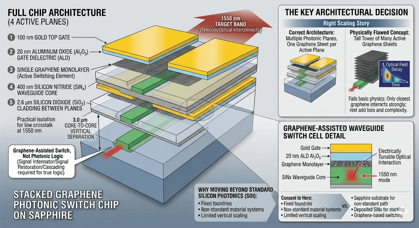
A stacked graphene photonic chip on sapphire designed for 1550 nanometer switching beyond standard silicon photonics
Photonics has advanced quickly by following a familiar path: standard silicon photonics built on silicon-on-insulator. That path has delivered real value, but it also locks designers into a narrow material system, a standard wafer stack, and process assumptions inherited from mainstream semiconductor manufacturing. For many applications that is fine. For new switching architectures, especially those that want vertical scaling and new active materials, it can become a constraint.
That is where this chip concept begins.
The design developed here is a stacked graphene-enabled photonic switch chip created specifically to move beyond standard silicon photonics while staying grounded in real fabrication logic. Rather than relying on a traditional silicon-on-insulator waveguide platform, this architecture uses a sapphire substrate, deposited silicon nitride waveguides, single graphene monolayers as active switch elements, 20 nanometer atomic layer deposited aluminum oxide gate dielectrics, and 100 nanometer gold top gates. The target operating band is 1550 nanometers, the most important wavelength range in telecom and optical interconnect systems.
This is not a fantasy rendering built from buzzwords. It is a first-pass chip concept shaped by physics, process limits, and practical material choices.
Why move beyond standard silicon photonics?
Silicon photonics became dominant for good reason. Silicon waveguides provide tight optical confinement, compact routing, and access to mature fabrication ecosystems. But silicon also comes with tradeoffs. It pushes the designer toward standard foundry flows, standard substrate structures, and standard process kits. That can be limiting when the goal is to experiment with multi-plane photonic stacks, graphene-based switching, and a non-standard integration path.
The goal here was not to reject silicon because it is bad. The goal was to avoid becoming trapped by a conventional process stack too early.
That is why the design moved toward deposited silicon nitride on sapphire. Silicon nitride is attractive because it is compatible with deposition-based fabrication, works well at 1550 nanometers, and opens the door to a more flexible, non-foundry-style build path. It does not confine light as tightly as silicon, but in exchange it offers a cleaner route for vertical stacking, material experimentation, and early-stage custom prototyping.
The key architectural decision
One of the biggest corrections in this concept was understanding what should and should not be stacked.
At first glance, it is easy to imagine that stacking many active graphene sheets vertically would create a stronger switch. That sounds good in a presentation, but it fails under basic physics. The optical field leaking out of a waveguide decays rapidly above the guide. That means only the graphene closest to the waveguide interacts strongly with the light. Higher graphene layers mostly add optical loss, electrostatic screening, contamination risk, and fabrication pain.
So the right architecture is not a tall tower of active graphene sheets.
The right architecture is multiple photonic planes, with one graphene layer per active plane.
That gives each switch plane its own waveguide, its own graphene switching sheet, and its own top gate. It also respects how optical modes actually behave.
The stack we settled on
The concept image and design discussion converged on a 4-plane active stack. Each plane contains the same basic switch unit:
- 100 nanometer gold top gate
- 20 nanometer aluminum oxide gate dielectric
- single graphene monolayer
- 400 nanometer silicon nitride waveguide core
- 2.6 micrometer silicon dioxide cladding between planes
- sapphire base substrate
The inter-plane spacing produces about 3.0 micrometers core-to-core vertical separation, which is a practical starting point for reducing unwanted coupling between photonic planes at 1550 nanometers.
This is important because the chip is not just a layered material stack. It is a vertical photonic architecture. The stack must keep each optical plane sufficiently isolated while still allowing multiple active planes in one footprint.
Why sapphire matters
Sapphire is not just there to make the chip sound exotic. It serves a real purpose.
A sapphire substrate gives the concept a strong, flat, thermally stable base that is not tied to the standard silicon photonics wafer model. It supports the idea of building the chip as a custom deposited structure rather than a strict foundry product. That matters because this concept is aimed at early sample development, not just fitting into an existing catalog process.
In practical terms, sapphire helps create room for a non-standard fabrication path while still giving the platform mechanical and thermal credibility.
What graphene is really doing
Graphene is the active switching material in this concept, but its role needs to be described honestly.
This is not graphene as decoration. It is not there just to make the chip sound advanced. The graphene monolayer is the electrically tunable optical element. When gated through the aluminum oxide dielectric and gold top gate, the graphene changes its optical interaction with the waveguide mode. In version one, the chip should be understood as a graphene-assisted waveguide switch or electro-optic modulation element, not yet as a full photonic logic computer.
That distinction matters. Real logic requires signal restoration, cascading strategy, and system-level architecture. A first sample chip needs to prove something simpler and more honest: that a graphene-controlled switch cell can work repeatably on a vertically integrated photonic platform.
Why vertical stacking is still valuable
Even after rejecting the idea of many graphene sheets in one tower, vertical stacking still remains central to the concept.
The reason is density.
A single photonic layer gives limited routing area. Multiple planes allow more functions, more switching elements, and more optical paths in the same chip footprint. In this design, stacking is used to create multiple active waveguide planes, not multiple graphene sheets fighting for the same evanescent field.
That is the right scaling story.
If the first plane works, additional planes can increase function density without pretending that impossible active stacking will somehow solve the problem.
What makes this chip concept credible
There are three reasons this design is worth taking seriously.
First, it respects field physics. The concept does not hide behind diagrams that imply unlimited vertical activity. It narrows the active layer to one graphene sheet per photonic plane.
Second, it respects fabrication reality. The stack assumes deposition, planarization, lithography, graphene transfer, dielectric growth, and gate metal formation. That is difficult, but it is real.
Third, it follows the right engineering sequence. A first chip does not need to prove the whole future. It needs to prove a switch cell, then a stacked switch platform, then repeatable fabrication.
That is how new hardware becomes real.
What a first sample should prove
A first sample chip based on this architecture should answer a few simple but decisive questions:
- Can the graphene switch be gated cleanly?
- What insertion loss does each active plane introduce?
- How much extinction ratio can be achieved at 1550 nanometers?
- Can multiple photonic planes coexist without excessive crosstalk?
- Can the fabrication flow be repeated with stable yield?
If those answers are strong, the design becomes more than an image. It becomes the foundation for a new class of stacked photonic switching chips built outside the assumptions of standard silicon photonics.
Conclusion
This chip concept represents a disciplined step into a different photonic future. It combines a sapphire substrate, deposited silicon nitride waveguides, graphene switching layers, atomic layer deposited aluminum oxide gate insulation, and a 4-plane vertical architecture designed for 1550 nanometer operation. It does not rely on fantasy scaling. It does not confuse stacked routing with stacked active graphene. And it does not pretend that a concept slide is already a product.
What it does offer is something more useful: a physically grounded, fabrication-aware path toward a new kind of stacked photonic switch platform.