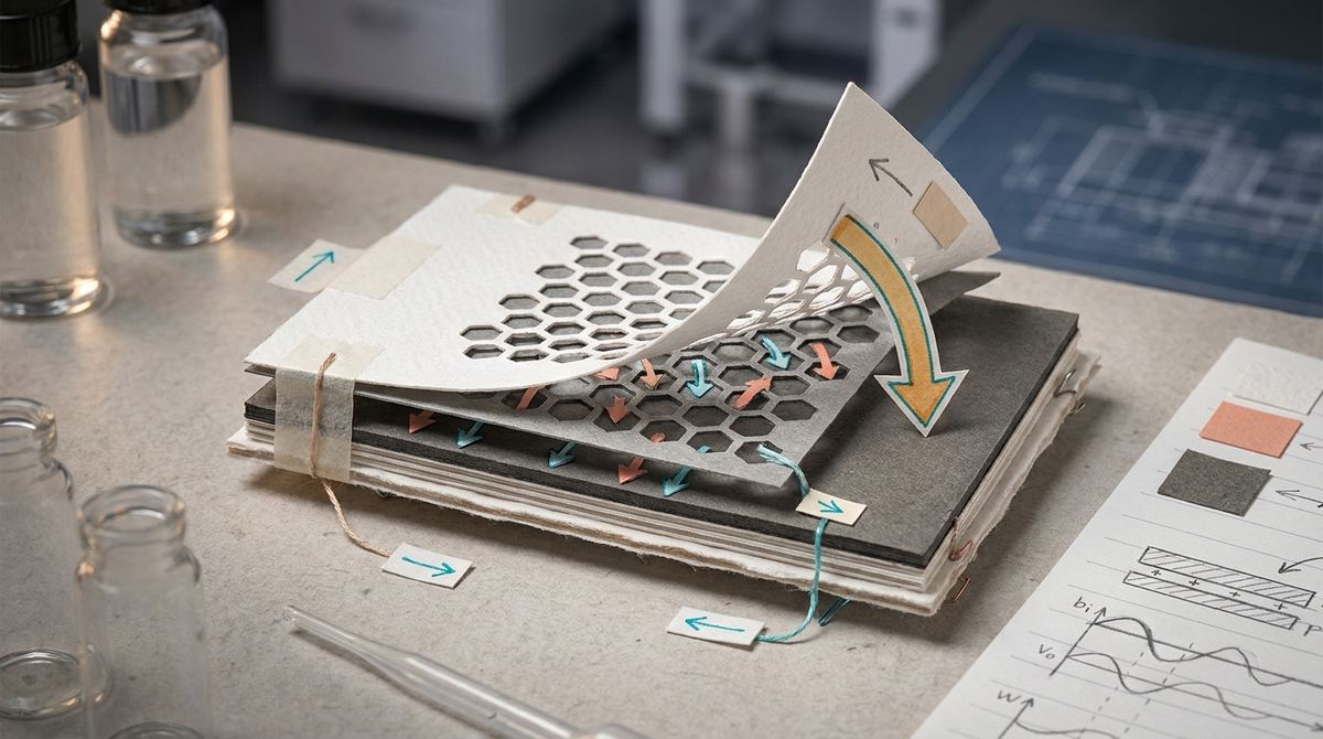
The quantum world is often described as a place of hidden patterns. In a standard material, electricity flows like water through a pipe, following a predictable path from one end to another. But in advanced two-dimensional materials like bilayer graphene, the electrons behave more like complex waves that can twist and turn in ways that defy classical logic. This twisting, a property known as topology, can protect quantum information from noise, making it a holy grail for future technologies. However, when we stack two sheets of material together, their electronic signals often blend into one. It is like trying to listen to a complex two-part harmony while standing too far away; you hear the melody, but you cannot distinguish the individual voices. To truly understand the music of the quantum world, we need a way to hear each layer separately.
The Problem This Research Is Solving
For decades, condensed matter physicists have struggled with the limitations of bulk measurement. When researchers study bilayer systems—which consist of two atomic layers stacked on top of each other—they typically measure the total current passing through the entire sandwich. While this provides valuable data about the material's overall conductivity, it acts as a mathematical average. This averaging effect is a significant obstacle because topological properties, such as the Chern number or Berry curvature, can manifest differently in the top layer compared to the bottom layer.
In many interesting quantum states, the topological signatures of the two layers might actually cancel each other out in a total measurement. For instance, if the top layer has a positive topological charge and the bottom layer has a negative one, a standard measurement would show a net charge of zero, leading a scientist to incorrectly conclude that the material has no interesting topological order. This "hidden topology" represents a massive blind spot in our ability to characterize the next generation of quantum materials. Without a way to isolate the signal from each individual sheet, we cannot fully map the landscape of electron movement in these complex, multi-layered architectures.
The Key Idea in Plain English
The breakthrough approach involves a technique called layer-resolved transport. Instead of simply passing electricity through the whole stack, researchers propose a method to probe the current flowing through each layer independently. By applying specific electrical potentials that target one layer more than the other, scientists can essentially peel back the layers of the measurement.
This is conceptually similar to using a high-powered microscope to look at the individual threads in a piece of woven fabric rather than just looking at the color of the whole cloth. By isolating the flow of electrons in the top sheet and comparing it to the flow in the bottom sheet, we can detect the subtle quantum "twists" that were previously hidden by the combined signal. This capability allows us to see if the topological order is distributed evenly, or if it is concentrated in a specific layer, providing a much more granular and accurate map of the material's quantum identity.
How the Graphene-Based System Works
To understand how this works, we must look at the physics of the bilayer interface. In a bilayer system, such as twisted bilayer graphene, the two sheets are not just sitting on top of each other; they are interacting through both electrostatic forces and quantum tunneling. This interaction causes the electron wavefunctions to overlap, creating a new set of energy levels that do not exist in a single layer.
When we talk about topology in this context, we are referring to the mathematical shape of these wavefunctions. In a topological insulator or a quantum Hall system, these wavefunctions have a specific "handedness" or twist. The layer-resolved transport method utilizes a sophisticated electrical setup where the top and bottom layers are contacted by different electrodes.
By controlling the voltage applied to the gates that sit above and below the graphene, researchers can manipulate the chemical potential of each layer separately. This allows them to drive a current through the top layer while keeping the bottom layer relatively inactive, or vice versa. When the current is driven in this way, the resulting voltage measured at the edges of the material becomes a direct probe of the topological properties of that specific layer. The relationship between the current and the resulting Hall voltage provides a direct measurement of the topological invariants, such as the Chern number, for that specific layer alone.
What the Researchers Found
In the theoretical framework explored by Hongquan Liu, J. I. A. Li, and D. E. Feldman, the researchers demonstrated that layer-resolved transport provides a definitive way to identify different types of topological orders. Their work shows that by measuring the current through individual layers, one can distinguish between various quantum states that appear identical in traditional bulk measurements.
Specifically, the research highlights how the distribution of topological charge across the layers can be mapped. They found that the current response in a single layer can reveal the presence of a non-zero Berry curvature, which is a key driver of the anomalous Hall effect. This means that even if the total material appears to be a simple conductor, the individual layers might be exhibiting profound topological phenomena. The study provides a mathematical and physical roadmap for how these measurements should behave, allowing experimentalists to know exactly what to look for when they build these complex devices in a laboratory setting.
Why the Result Matters
The implications of being able to resolve layer-specific transport are profound for the field of quantum materials. The primary reason this matters is the quest for fault-tolerant quantum computing. One of the biggest challenges in quantum computing is "decoherence," where the fragile quantum state of a qubit is destroyed by thermal noise or environmental interference.
Topological quantum computing seeks to solve this by storing information in the "twists" of the electron wavefunctions rather than in the position or spin of a single electron. Because these twists are global properties of the material, they are naturally protected from local disturbances. If we want to build these computers, we must first be able to create and verify these topological states. Layer-resolved transport provides the diagnostic tool necessary to confirm that a material has the correct topological order to function as a quantum memory or a quantum logic gate. Without this ability to probe the layers, we are essentially flying blind in the search for the perfect quantum substrate.
Limitations and What Still Needs Testing
While this research offers a powerful theoretical framework, it is important to recognize that we are still in the early stages of experimental realization. Implementing layer-resolved transport is an immense engineering challenge. To work effectively, the contacts used to touch the top and bottom layers must be extremely precise and isolated from one another. In most current manufacturing processes, creating such selective contacts without causing "leakage" between the layers is incredibly difficult.
Furthermore, these quantum effects are often only visible at extremely low temperatures, near absolute zero. At higher temperatures, thermal energy causes electrons to jump erratically between layers, which "blurs" the topological signals and makes layer-specific measurements nearly impossible. There is also the issue of material perfection. Any defect, impurity, or wrinkle in the graphene layers can disrupt the delicate quantum interference patterns required for topological order, potentially masking the very signals the researchers are trying to probe. Therefore, while the theory is robust, the transition from the mathematical model to a practical, room-temperature device remains a significant hurdle.
Real-World Applications
The journey from a theoretical physics paper to a consumer product is long, but the roadmap for layer-resolved transport points toward several transformative technologies. The most immediate application lies in the development of advanced sensors. Materials with specific topological properties can be used to create sensors that are incredibly sensitive to magnetic fields or electric fields, which could lead to more accurate medical imaging devices or highly sensitive geological exploration tools.
In the realm of electronics, the ability to control and measure the properties of individual layers could lead to the development of "topological transistors." These would be a new class of switches that operate with much lower power consumption and much higher speeds than current silicon-based transistors. Because the topological states are protected, these devices would be less prone to the heat generation that currently limits the speed of modern computer processors. Ultimately, this research acts as a foundational step toward the era of topological electronics, where the very structure of the material dictates the efficiency and reliability of the device.
If You Remember One Thing
If you take away only one concept from this research, let it be this: the true potential of advanced materials is often hidden within their individual layers, and we need new ways to "listen" to those layers to unlock the next generation of quantum technology.
FAQ
What exactly is topological order in a material?
Topological order refers to a special way that particles like electrons organize themselves so that their behavior is determined by the mathematical shape of their quantum wavefunctions. Unlike regular materials where electrons move based on local forces, electrons in a topologically ordered state move in ways that are defined by the overall global structure of the material. This makes their properties very stable and resistant to small disturbances or impurities.
Why can't we just use standard electrical measurements?
Standard electrical measurements typically look at the total current flowing through a whole sample. In a multi-layered material, the signals from the top and bottom layers are combined into a single value. Because some topological properties can be positive in one layer and negative in another, they can cancel each other out in a total measurement, making an interesting material appear completely ordinary.
How does layer-resolved transport solve this problem?
Layer-resolved transport uses specialized electrical contacts and voltage controls to isolate the current flowing through one layer from the other. By targeting a single layer, researchers can see its unique quantum signature without the interference or cancellation from the other layers. This effectively allows us to see the "hidden" quantum properties that a standard measurement would miss.
Is this research going to lead to quantum computers soon?
Not immediately. While this research is a critical step toward building the components for quantum computers, we still face significant engineering challenges. We need to be able to manufacture these layers with perfect precision and operate them at temperatures that are more practical than the extreme cold currently required. This research provides the blueprint, but the construction is still in the early stages.
What is the role of graphene in this specific research?
Graphene is a two-dimensional material made of a single layer of carbon atoms. Because it is so thin, it is the perfect playground for studying quantum effects. When two layers of graphene are stacked, their interaction creates the complex, tunable electronic environments that researchers want to probe using layer-resolved transport.
Conclusion
The work conducted by Hongquan Liu, J. I. A. Li, and D. E. Feldman represents a vital advancement in our understanding of two-dimensional materials. By providing a method to distinguish between the individual topological identities of layers in a bilayer system, this research moves us closer to mastering the complexities of the quantum world. While the engineering challenges of implementing layer-resolved transport are significant, the potential rewards—ranging from ultra-efficient electronics to stable quantum computers—make this a fundamental frontier in modern physics. As we refine our ability to probe the hidden layers of matter, we unlock the door to a new era of technological capability.