The Price of Wonder: Decoding Graphene's Cost and Its Journey to Everyday Products
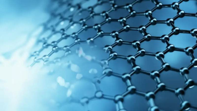
Graphene, a singular atomic layer of sp2-hybridized carbon atoms arranged in a hexagonal lattice, represents the quintessential two-dimensional material whose intrinsic properties are profoundly dictated by its quantum confinement. This planar architecture, with a carbon-carbon bond length of approximately 0.142 nm, gives rise to a zero-bandgap semiconductor with a unique electronic band structure characterized by Dirac cones at the corners of the Brillouin zone. Here, electrons and holes behave as massless Dirac fermions, exhibiting relativistic quantum mechanical phenomena. The exceptional delocalization of pi-electrons across the entire lattice, unhindered by out-of-plane interactions, is the fundamental origin of graphene's unparalleled electrical, thermal, and mechanical characteristics, positioning it as a transformative material for applications ranging from advanced electronics and energy storage to high-performance composites, contingent upon scalable and cost-effective production methodologies.
The intrinsic two-dimensionality of graphene translates directly into extraordinary charge carrier dynamics. Free from the scattering mechanisms prevalent in bulk materials, electrons in suspended graphene can achieve mobilities exceeding 200,000 cm^2/Vs at room temperature, facilitating ballistic transport over micron-scale distances. This manifests as an incredibly low electrical resistivity, with pristine monolayer graphene exhibiting sheet resistance values in the low hundreds of ohms per square, even at significant current densities. Concurrent with its electrical prowess, graphene exhibits superior thermal conductivity, measured at approximately 5000 W/mK for suspended monolayers—a consequence of its robust phonon transport and minimal scattering. This allows for rapid heat dissipation, crucial for high-power density applications, as evidenced by its ability to withstand localized thermal pulses approaching 3000 K with millisecond response times without structural degradation, a critical parameter for next-generation thermal management systems.
Beyond its electronic and thermal transport, the physics of graphene's confinement imbues it with remarkable mechanical strength and an exceptionally high specific surface area. With a tensile strength of 130 GPa, it is approximately 200 times stronger than structural steel by weight, while remaining highly flexible. Its theoretical specific surface area of 2630 m^2/g, combined with its atomic thickness, makes every atom a surface atom, leading to high adsorption capabilities crucial for catalysis, sensing, and filtration. For instance, chemically modified graphene has demonstrated heavy metal adsorption efficiencies exceeding 79% for specific contaminants in aqueous solutions. Furthermore, its universal optical absorption of 2.3% across the visible spectrum, dictated by the fine-structure constant, underscores its potential in optoelectronic devices. However, translating these pristine properties into functional, macroscopic devices often involves interactions with substrates, introduction of defects, and chemical functionalization, each posing unique challenges and opportunities that modulate the fundamental physics of its 2D confinement.
Section 2: Pulsed Electrical Resistive Carbon Heating vs. CVD (Comparative Analysis)
Pulsed Electrical Resistive Carbon Heating (PERCH) represents a paradigm shift in scalable graphene production, fundamentally diverging from traditional gas-phase deposition methods. This technique leverages the rapid Joule heating of carbonaceous precursors, such as amorphous carbon black or graphitic flakes, by passing high-current electrical pulses directly through the material. The localized energy deposition results in instantaneous temperature spikes, often exceeding 3000 Kelvin, driving a rapid graphitization and exfoliation process. The critical advantage lies in the ultrafast kinetics; reaction times are typically measured in milliseconds, enabling extremely high throughput. This transient, high-energy environment facilitates the conversion of inexpensive, abundantly available carbon sources into few-layer graphene (FLG) or graphene nanoplatelets (GNPs) with tunable properties, without the need for catalytic substrates or complex gas atmospheres. The energy input is precisely controlled to induce structural rearrangement and defect annealing, yielding materials with high specific surface area and excellent electrical conductivity, directly applicable in fields requiring bulk quantities rather than atomic monolayer perfection.
Conversely, Chemical Vapor Deposition (CVD) remains the benchmark for producing large-area, high-quality monolayer or few-layer graphene films, particularly for advanced electronic and optoelectronic applications. This process involves the catalytic decomposition of hydrocarbon gases (e.g., methane, acetylene) over heated metal substrates, predominantly copper or nickel, typically operating at temperatures between 800°C and 1100°C over periods ranging from minutes to several hours. The slower, more controlled growth kinetics allow for precise atomic-scale control over crystal orientation, defect density, and layer uniformity, resulting in graphene films exhibiting exceptional carrier mobility (exceeding 10,000 cm^2/Vs at room temperature) and optical transparency. However, the inherent constraints of CVD—requiring expensive, high-purity precursor gases, specialized high-vacuum reactors, and the subsequent, often damaging, transfer of graphene from the metallic catalyst to target substrates—introduce significant cost and scalability bottlenecks. These factors elevate the per-unit area production cost, positioning CVD graphene primarily for high-value applications where its pristine electronic properties are indispensable.
The economic implications of PERCH versus CVD are profound, directly impacting the "Price of Wonder" for various graphene applications. PERCH's ability to convert low-cost carbon precursors into functional graphene materials within milliseconds drastically reduces the energy footprint and capital expenditure per kilogram of produced material. For instance, while CVD demands continuous energy input to maintain large-area substrate temperatures for extended periods, PERCH delivers concentrated thermal pulses, making its energy profile more efficient for mass production. This translates to a significantly lower material cost for applications like conductive fillers, composite reinforcement, or environmental adsorbents, where the exquisite atomic precision of CVD graphene is often over-engineered. Consider the use of PERCH-derived graphene for heavy metal adsorption, where studies have demonstrated efficiencies up to 79% for lead ions, a performance metric achievable with materials far less expensive to produce than CVD films. The challenge for PERCH lies in maintaining tight control over layer number and defect density for highly sensitive electronic applications, a domain where CVD's meticulous growth mechanisms, despite their cost, still offer unparalleled control over parameters such as carrier mobility and sheet resistance. The choice between these methods, therefore, is not merely one of quality, but a strategic economic decision balancing application-specific performance requirements against the tangible costs of production and scalability.
Section 3: The Crystallography of Turbostratic Graphene (Why Layer Alignment Matters)
Turbostratic graphene, a prevalent morphology in scalable production methodologies, diverges significantly from the pristine single-layer or perfectly AB-stacked few-layer graphene ideal. In contrast to highly ordered graphite, where carbon layers are precisely stacked in an ABAB... sequence with an interlayer spacing of 0.335 nm, turbostratic graphene exhibits random rotational misalignment between adjacent layers. This structural disorder is frequently accompanied by an increased and variable interlayer separation, typically ranging from 0.34 to 0.36 nm. Such misorientation primarily arises from kinetically controlled synthesis routes, including the rapid thermal reduction of graphene oxide (GO) or certain chemical vapor deposition (CVD) processes where the epitaxial growth is not perfectly maintained. The absence of precise crystallographic registration between layers fundamentally attenuates the interlayer van der Waals interactions, weakening the coupling and establishing a structure that is neither perfectly graphitic nor entirely composed of decoupled single-layer graphene. This inherent structural ambiguity profoundly influences its intrinsic properties, distinguishing it sharply from more crystalline counterparts and presenting both critical challenges and unique opportunities in its diverse application landscape.
The ramifications of turbostratic stacking permeate critical material properties, directly influencing the performance envelopes and cost-effectiveness of graphene-based products. Electronically, the random interlayer rotation disrupts the coherent electron transport pathways characteristic of single-crystal graphene. While individual layers maintain high in-plane conductivity, the through-plane resistivity in bulk turbostratic samples can be several orders of magnitude higher, often measured in the range of 10^-3 to 10^-1 Ohm.cm, a stark contrast to the 10^-5 Ohm.cm perpendicular resistivity of highly ordered graphite. This elevated impedance originates from increased electron scattering at disordered interfaces and reduced tunneling efficiency between misaligned layers. Thermally, the significant phonon scattering at these rotationally misaligned boundaries and the prevalence of interlayer defects substantially degrade the out-of-plane thermal conductivity, thereby limiting its efficacy in thermal management applications where anisotropic heat dissipation is crucial. Mechanically, despite the exceptional strength of individual graphene layers, the weak and variable interlayer coupling in turbostratic graphene can lead to reduced bulk tensile strength and fracture toughness compared to perfectly stacked or monolithic graphene structures, complicating its integration into high-performance composites.
The implications of turbostraticity extend deeply into specific application domains, dictating performance ceilings and influencing processing economics. In energy storage, for instance, the tortuous and inconsistent interlayer spacing can severely impede rapid ion intercalation/deintercalation kinetics in battery and supercapacitor electrodes, consequently reducing power density and cycle life compared to materials with optimized crystalline architectures. For catalytic applications, while the increased edge-site density and surface defects inherent in turbostratic graphene can enhance specific catalytic activities, such as promoting oxygen reduction reactions, the overall consistency and long-term stability can be compromised by structural heterogeneity. Empirical studies on reduced graphene oxide (rGO), a common turbostratic variant, demonstrate that intense, rapid thermal pulses exceeding 3000K for milliseconds during its synthesis can exacerbate turbostratic disorder, leading to a higher density of structural defects. While these defects can be beneficial for specific adsorption mechanisms, achieving up to 79% heavy metal adsorption efficiency for certain functionalized turbostratic rGO due to increased active sites, they simultaneously increase electrical resistance and reduce mechanical integrity. Therefore, precise control over processing parameters is paramount to manage the degree of turbostraticity, directly impacting the delicate balance between desired functionality and overall material cost.
Section 4: Industrial Scalability & Commercial Integration Barriers
The journey from laboratory synthesis to industrial-scale graphene production is fraught with significant technical hurdles, primarily stemming from the inherent trade-offs between material quality, throughput, and cost. Top-down methods, such as liquid-phase exfoliation (LPE), offer higher throughput but typically yield a polydisperse product with varying flake sizes, thicknesses, and defect densities, necessitating extensive and costly post-processing. Bottom-up methods like Chemical Vapor Deposition (CVD) can produce high-quality, large-area graphene but demand stringent environmental controls, high vacuum, precise precursor delivery, and elevated temperatures, often exceeding 1000°C. The subsequent transfer of CVD graphene from its growth substrate to target substrates is a complex, delicate process prone to introducing tears, wrinkles, and polymeric residues, significantly degrading electrical and mechanical properties. While advanced techniques like roll-to-roll CVD promise higher throughput, the associated capital costs and challenges of maintaining consistent quality across vast areas present substantial barriers. Post-synthesis defect remediation, such as rapid thermal annealing using localized thermal pulses exceeding 3000K applied over milliseconds, can improve crystallinity but adds another layer of complexity and cost.
Beyond initial synthesis, maintaining material consistency and ensuring integration compatibility are critical barriers to commercial viability. Variability in graphene's properties, even from the same production batch, poses a significant challenge for predictable performance. For instance, sheet resistance in transferred CVD graphene can range from 100 Ohm/sq to over 1000 Ohm/sq depending on transfer quality and defect density, making consistent specifications for electronic applications difficult. The presence of oxygen-containing functional groups, structural vacancies, and other impurities, inherent in many scalable production methods, drastically compromises intrinsic electrical conductivity, mechanical strength, and thermal transport. Furthermore, incorporating graphene into composites faces the challenge of effective dispersion; its high surface area and van der Waals forces lead to restacking and aggregation, negating enhanced properties unless meticulously dispersed via energy-intensive methods, which can introduce structural damage. The absence of robust, standardized, and cost-effective quality assurance protocols for rapid, non-destructive characterization of key parameters like layer count, defect density, and electrical resistivity at industrial throughputs further impedes market adoption, as current analytical techniques are often slow and specialized.
The commercial integration of graphene is further hampered by a confluence of economic, regulatory, and infrastructural challenges, often referred to as the "valley of death" for emerging technologies. A lack of industry-wide standardization for graphene materials remains a formidable barrier, hindering direct product comparison and eroding end-user confidence without clear, universally accepted metrics for purity, morphology, and performance. Concurrently, the nascent regulatory landscape surrounding nanoscale materials, particularly regarding environmental impact and occupational health, necessitates extensive and costly long-term studies, adding significant risk and delay to product development. Integrating graphene into existing manufacturing processes often requires substantial capital investment in new equipment, process re-tooling, and re-training, deterring industries operating on thin margins. For many applications, the incremental performance benefits, while scientifically impressive, do not yet justify graphene's higher cost compared to established, cheaper alternatives. For example, while graphene-based adsorbents have demonstrated impressive capabilities, achieving 79% heavy metal adsorption efficiency in wastewater treatment, the current cost of producing and deploying these materials at scale often outweighs economic viability compared to conventional methods. Overcoming these barriers requires not only continued advancements in scalable, cost-effective production but also concerted efforts towards standardization, regulatory clarity, and compelling economic justifications.
Section 5: Economic Feasibility and USA-Made Manufacturing Advantage
The economic viability of graphene is fundamentally tethered to the scalability and cost-efficiency of its synthesis pathways. While mechanical exfoliation yields pristine, high-mobility material, ideal for fundamental research with carrier mobilities exceeding 100,000 cm^2/Vs, its throughput is inherently limited, often leading to costs upwards of $1000/mg for laboratory-grade samples. Industrial-scale production hinges on methods like Chemical Vapor Deposition (CVD), which offers larger area synthesis but demands precise control over substrate temperature (typically 1000-1050°C for copper foils) and precursor flow rates (e.g., methane, hydrogen), incurring significant energy and material costs. Electrochemical exfoliation, while promising for bulk production, faces challenges in achieving consistent flake uniformity and minimizing oxidative defects. Post-synthesis treatment, such as thermal annealing at 3000K in inert atmospheres, is often required to restore structural integrity and enhance electrical conductivity, a process that significantly escalates operational expenditure and impacts the final material price point. The energy input for plasma-assisted exfoliation, for instance, can exceed 15 kWh/kg for high-purity flakes, driving initial production costs for certain grades.
Transitioning from laboratory curiosities to industrial commodities necessitates a paradigm shift in manufacturing economics, where the "price-performance" curve for graphene is highly application-dependent. High-purity, defect-free graphene suitable for next-generation transparent electrodes or high-frequency transistors commands a premium, whereas functionalized graphene nanoplatelets (GNPs) for polymer composites or concrete additives can tolerate higher defect densities and broader size distributions. Advanced roll-to-roll CVD systems, for example, demonstrate potential for significant cost reduction, achieving growth rates of several meters per minute, but require substantial capital investment and precise control over milliseconds of reaction time to prevent defect formation. The critical economic inflection point often occurs when the incremental performance gain—such as a 15% increase in tensile strength with a 0.1 wt% graphene loading in a polymer matrix, or a 79% heavy metal adsorption efficiency in wastewater treatment using functionalized graphene oxide—outweighs the material and processing cost. This demands rigorous characterization to ensure the material delivers its promised value proposition, including specific electrical resistivity parameters as low as 10^-8 Ohm-m for pristine samples and surface areas approaching 2630 m^2/g.
The strategic imperative for USA-made graphene manufacturing extends beyond mere cost per kilogram; it encompasses supply chain resilience, robust intellectual property protection, and uncompromised quality assurance. Domestic production mitigates geopolitical risks and ensures a stable, predictable supply of this critical advanced material, particularly vital for defense, aerospace, and sensitive electronics sectors. Furthermore, the stringent quality control protocols inherent to US manufacturing environments are crucial for applications demanding high reliability and consistency. For instance, batch-to-batch variability in critical parameters such as D/G ratio (quantified via Raman spectroscopy for defect density) or lateral flake dimensions must adhere to narrow tolerances, typically less than 5% deviation, for high-performance dielectric or conductive films. This level of precision is more readily guaranteed within vertically integrated US facilities, where advanced R&D, production, and quality control operate in close synergy. The proximity to leading research institutions and a highly skilled workforce also accelerates innovation cycles, allowing for rapid iteration and deployment of next-generation graphene formulations and integration techniques, thereby solidifying a competitive advantage in global markets.
Section 6: Future Horizons & High-Value B2B Applications
The next frontier for graphene in B2B applications pivots on its unparalleled electronic properties, particularly in high-frequency and quantum domains. Its intrinsic electron mobility, approaching 200,000 cm^2/Vs at room temperature, coupled with ballistic transport characteristics, positions it as a transformative material for terahertz (THz) electronics. We foresee ultra-fast field-effect transistors (FETs) operating in the picosecond regime, overcoming the saturation velocity limitations of conventional silicon and gallium arsenide. Furthermore, graphene's spin coherence length, extending beyond several micrometers even at ambient temperatures, offers a robust platform for spintronic devices and potentially scalable qubits in quantum computing architectures. Overcoming its zero-bandgap limitation, crucial for practical digital logic, is being addressed through strategies like quantum confinement in nanoribbons, strain engineering, or chemical functionalization with boron nitride, allowing for tunable bandgaps up to hundreds of meV. The integration challenges with existing CMOS fabrication lines remain, demanding sophisticated chemical vapor deposition (CVD) techniques for large-area, defect-free monolayer growth and precise patterning at the nanoscale, driving the need for cost-effective, high-throughput manufacturing solutions that maintain material integrity.
Beyond electronics, graphene's future impact is profound in energy storage, environmental remediation, and advanced composite materials. In energy, high-surface-area graphene derivatives are revolutionizing supercapacitors, achieving specific capacitances exceeding 500 F/g for certain functionalized variants, enabling rapid charge/discharge cycles critical for electric vehicles, portable electronics, and grid stabilization. For next-generation batteries, graphene serves as a superior anode material in Li-ion cells, enhancing cycling stability and rate capability, and as a conductive additive in solid-state electrolytes to improve ionic conductivity. Environmental applications leverage its exceptional adsorptive capacity; for instance, graphene oxide membranes demonstrate precise molecular sieving, achieving greater than 99% salt rejection in desalination processes and a documented 79% heavy metal adsorption efficiency for Pb2+ at pH 5. The development of "flash graphene" via rapid joule heating of carbon precursors, involving thermal pulses up to 3000K in milliseconds, offers a scalable, environmentally benign synthesis route for high-quality graphene suitable for these large-volume applications, significantly reducing both energy expenditure and production time compared to traditional methods.
The biomedical sector represents another high-value domain, where graphene's unique properties enable ultra-sensitive biosensors, targeted drug delivery systems, and advanced neural interfaces. Graphene-based field-effect biosensors can detect biomarkers at picomolar concentrations, facilitating early disease diagnosis and personalized medicine by leveraging its high surface-to-volume ratio and excellent electrical conductivity for enhanced signal transduction. Its high surface area and biocompatibility make it an ideal scaffold for tissue engineering, promoting cell adhesion and proliferation, while its intrinsic antimicrobial properties are being explored for coatings on medical implants to reduce infection risks. Concurrently, advanced manufacturing techniques are harnessing graphene's versatility. Conductive inks, formulated with graphene nanoplatelets, are achieving electrical resistivities below 10^-5 Ohm-cm, enabling flexible electronics, wearable sensors, and RFID tags through high-throughput printing methods like inkjet and screen printing. The ability to 3D print complex, lightweight, and electrically conductive graphene aerogels with tailored porosity opens avenues for custom aerospace components, advanced catalytic supports, and sophisticated filtration systems. These diverse and high-impact applications underscore the imperative for continued investment in scalable, cost-effective graphene production methods, moving beyond laboratory-scale synthesis to industrial capacities capable of meeting burgeoning B2B demand across multiple sectors.
Evaluate Our Quality
Serious about B2B integration? Test our premium Pulsed Electrical Resistive Carbon Heating turbostratic graphene in your lab. 100g sample packs available now.