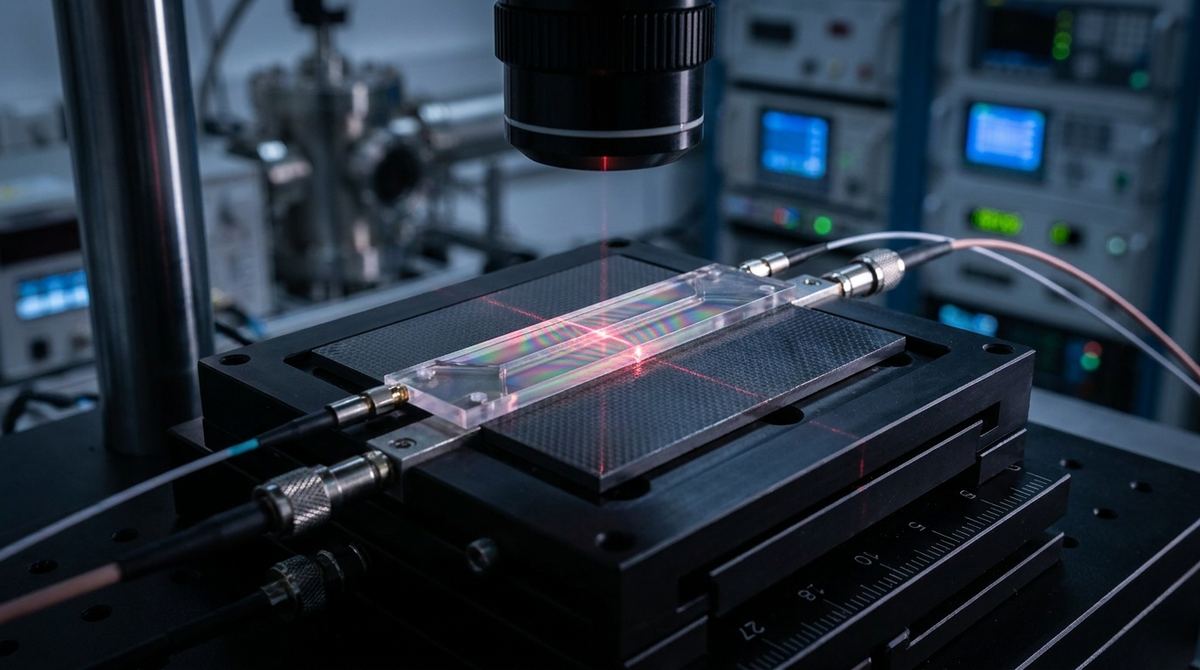
Overview of the Plasmonic Modulator Concept
Graphene is a premier candidate for infrared (IR) photonics because it supports surface plasmon polaritons (SPPs) at much lower frequencies than traditional metals. However, graphene is notoriously sensitive to its environment. Ambient moisture and oxygen cause uncontrolled doping, which leads to device drift and unreliable performance. To build a commercially viable infrared modulator or sensor, you must be able to lock in the electronic properties of the graphene.
The research by Chi et al. (2026) demonstrates that using ultrathin oxide overlayers—specifically Molybdenum Oxide (MoOx) and Zinc Oxide (ZnOx)—allows for systematic engineering of graphene plasmons through interfacial charge transfer. By depositing these oxides via Physical Vapor Deposition (PVD), you can increase the carrier density of the graphene, which in turn tunes the plasmonic wavelength and improves the signal-to-noise ratio. This method also provides a way to stabilize the device against ambient degradation for several months.
This guide outlines how to build a prototype of a tunable IR plasmonic modulator using these oxide-graphene heterostructures.
Required Materials and Equipment
To build a functional prototype, your lab will require the following:
1. Graphene: High-quality CVD-grown graphene transferred onto a silicon/silicon dioxide (SiO2/Si) substrate.
2. Molybdenum Oxide (MoOx): High-purity target for Physical Vapor Deposition (PVD).
3. Zinc Oxide (ZnOx): High-purity target for PVD, used to tune the response back toward the original state.
4. Deposition System: A vacuum-based PVD system (such as an electron-beam evaporator or a thermal evaporator) capable of sub-nanometer precision.
5. Characterization Tools: A Raman spectrometer (to verify doping levels) and an infrared source/detector setup.
6. Cleaning Agents: Acetone, Isopropanol, and Deionized (DI) water for substrate preparation.
7. Quartz Crystal Microbalance (QCM): Essential for monitoring sub-nanometer deposition rates.
Prototype Fabrication Workflow
The success of this device depends entirely on the precision of the oxide layer thickness. The research indicates that the most significant charge transfer occurs at sub-nanometer thicknesses.
Step 1: Substrate Preparation. Clean your SiO2/Si substrate using a standard RCA cleaning process or a sequence of acetone, isopropanol, and DI water. The surface must be completely dry and free of any organic contaminants to ensure the oxide makes direct contact with the graphene.
Step 2: Graphene Transfer. Transfer your CVD graphene onto the substrate using a standard polymer-assisted transfer method. Once the transfer is complete, perform a thermal anneal. We recommend a temperature range of 300 to 400 degrees Celsius in a vacuum or a hydrogen/argon atmosphere. This step is critical to remove polymer residues that would otherwise block the interfacial charge transfer.
Step 3: MoOx Deposition. Using your PVD system, deposit a very thin layer of MoOx. Based on the research, the charge-transfer doping increases rapidly at sub-nanometer thicknesses. For your first prototype, we suggest a starting thickness range of 0.5 nm to 2.0 nm. You must use a QCM to monitor the deposition in real-time to ensure you do not overshoot this range.
Step 4: ZnOx Capping (Optional). If the MoOx doping is too aggressive for your specific application, you can deposit a layer of ZnOx. The research shows that ZnOx can partially reverse the effects of MoOx, allowing you to fine-tune the carrier density to your exact requirements.
Step 5: Stabilization Layer. The research suggests that a 3-nm-thick MoOx overlayer stabilizes the plasmonic response for at least seven months under ambient conditions. For your prototype, aiming for this 3-nm thickness will provide the necessary environmental protection.
Testing and Characterization Protocol
Since most small labs and startups do not have access to Scanning Near-field Optical Microscopy (SNOM), you must use proxy measurements to validate your prototype.
1. Raman Spectroscopy: This is your most important tool for verifying doping. An increase in carrier density due to MoOx doping will cause a blue shift (a shift toward higher frequencies) in the graphene G-peak. The magnitude of this shift will allow you to quantify the level of charge transfer achieved.
2. Electrical Conductivity: Use a four-probe setup to measure the sheet resistance of the graphene. The MoOx layer should significantly decrease the resistance by increasing the carrier density.
3. Infrared Response: If you have access to an IR microscope or an FTIR spectrometer, observe the absorption spectrum. The goal is to see a shift in the plasmonic resonance frequency that corresponds to the new carrier density.
4. Electrostatic Gating: You can further modulate the carrier density using an external electrostatic gate. Note that the response may be nonlinear, as suggested by the research, due to the gate-dependent interfacial charge redistribution.
Engineering Assumptions and Critical Parameters
The following details are engineering assumptions derived from the research findings to assist in your implementation:
1. Thickness Control: The research highlights that charge transfer is highly sensitive to thickness, especially below 1 nm. We assume that a standard laboratory PVD system with a QCM can achieve the necessary precision, but this remains the primary technical challenge.
2. Deposition Temperature: The research does not specify the exact temperature during deposition. We assume room temperature deposition is sufficient, provided the vacuum quality is high.
3. Stability: The research claims 7 months of stability for a 3-nm MoOx layer. We assume this stability is dependent on the vacuum quality during the deposition process and the hermeticity of the oxide layer.
4. Doping Direction: We assume the MoOx acts as a p-type dopant (electron withdrawer) and ZnOx acts as an n-type dopant (electron donor) relative to the graphene.
Risk Assessment and Mitigation
1. Risk: Non-uniform oxide deposition.
Problem: If the MoOx layer is not uniform across the graphene surface, the plasmonic response will vary, leading to signal noise and inconsistent device performance.
Mitigation: Use a rotating substrate during PVD and optimize the deposition rate to be extremely slow (e.g., 0.1 Angstroms per second) to ensure coverage uniformity.
2. Risk: Graphene degradation during transfer.
Problem: Micro-cracks or polymer residue can prevent the oxide from making direct contact with the graphene, negating the charge transfer mechanism.
Mitigation: Use high-quality PMMA transfer methods and ensure a thorough thermal anneal step before deposition.
3. Risk: Over-doping.
Problem: Too much MoOx might make the graphene too conductive or change its optical properties too drastically for your specific sensor application.
Mitigation: Start with extremely thin layers (e.g., 0.2 nm) and incrementally increase thickness until the desired plasmonic wavelength is achieved.