The Challenge of Ion-Based Computing
In traditional semiconductor memory, we rely on the movement of electrons to represent bits. While efficient, electronic memory faces fundamental scaling limits and high power consumption in certain neuromorphic applications. Ion-based computing offers a compelling alternative because ions are much larger and slower than electrons, allowing for non-volatile states that mimic the synaptic plasticity of the human brain.
However, there is a major engineering hurdle in standard ion-based devices: the coupling of density and transport. In a typical single-gate device, if you apply a voltage to change the number of ions (the density), you also inadvertently change how fast those ions move (the transport rate). This makes it extremely difficult to set a stable memory state without causing a massive, uncontrolled current surge or a drift in the state.
Recent research has demonstrated a way to break this limitation using double-gated van der Waals (vdW) heterostructures. By using two gates—a top gate and a back gate—we can decouple these two variables. We can use one gate to set a fixed ionic density (the memory state) and the second gate to control the rate at which ions move (the switching speed). This enables a hybrid ionic-electronic transistor that can perform logic operations and retain memory with an ON/OFF ratio exceeding two orders of magnitude.
The Prototype Concept
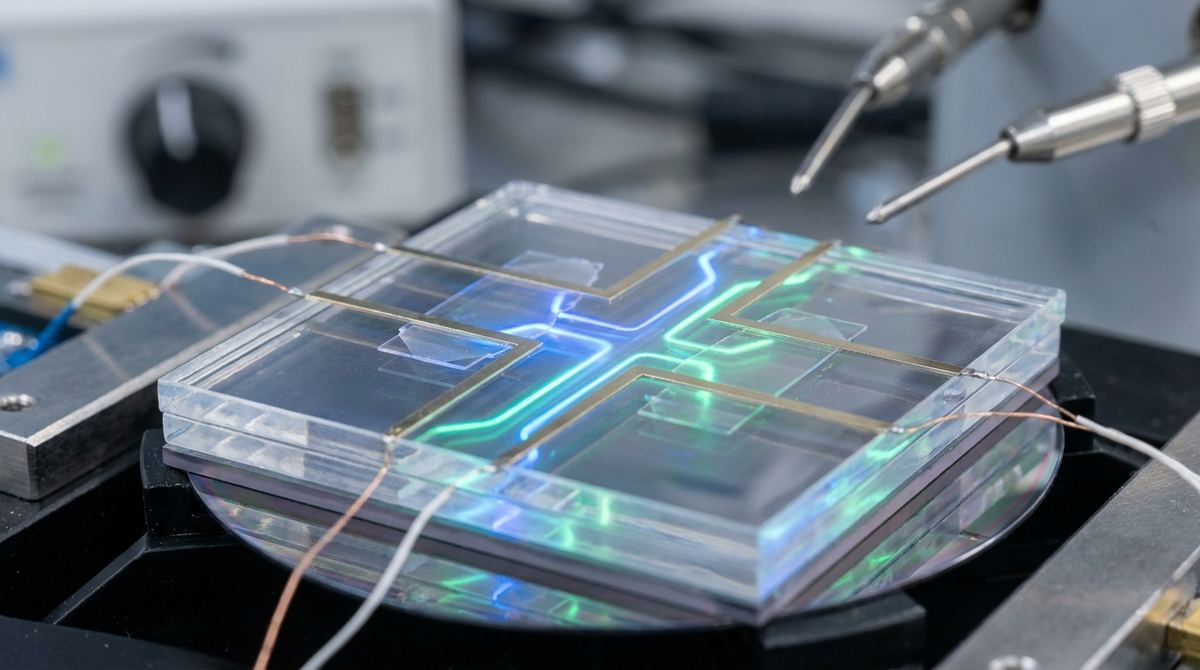
The goal for a lab-scale prototype is to create a hybrid device where a graphene channel is sandwiched between insulating layers and an electrolyte, allowing for precise control over Li+ ion distribution.
The target application for this prototype is a non-volatile, multi-state memory cell. Unlike a standard binary switch, this device can occupy discrete ionic-density states. These states are marked by specific plateaus in the electronic response of the graphene, allowing for multi-level cell (MLC) storage, which is essential for neuromorphic computing and high-density memory.
Required Materials and Equipment
To build this device, you will need access to a cleanroom environment capable of handling van der Waals heterostructure assembly.
1. Graphene: High-quality monolayer graphene (CVD-grown or mechanically exfoliated).
2. Hexagonal Boron Nitride (hBN): High-quality flakes for insulation and dielectric layers.
3. Lithium Salt Electrolyte: A solution of LiPF6 or LiClO4 in an organic solvent (such as acetonitrile) or a solid-state polymer electrolyte.
4. Substrate: A heavily doped Silicon/SiO2 substrate, which will serve as the back gate.
5. Electrodes: Gold (Au) or Platinum (Pt) for the source and drain contacts.
6. Top Gate: A conductive layer (like a thin metal film or a second graphene sheet) separated from the electrolyte by a thin dielectric.
7. Equipment: An AFM (Atomic Force Microscope) for layer stacking, a probe station for electrical characterization, and a spin-coater if using liquid electrolytes.
Prototype Assembly Steps
Building a van der Waals heterostructure requires extreme precision. The following steps assume a standard mechanical transfer method.
1. Substrate Preparation: Clean your Si/SiO2 substrate using standard RCA cleaning procedures to ensure no organic contaminants interfere with the layer stacking.
2. Bottom Dielectric Layer: Deposit or transfer a thin layer of hBN onto the substrate. This layer acts as the primary insulator between the silicon back gate and the graphene channel. For a functional device, we assume a thickness of 10 to 20 nm.
3. Graphene Channel: Transfer a monolayer of graphene onto the hBN layer. Ensure the graphene is continuous and free of wrinkles, as wrinkles can cause local variations in ion density.
4. Protection/Insulation Layer: Transfer a second layer of hBN onto the graphene. This layer protects the graphene from direct contact with the electrolyte and provides the necessary electrostatic coupling. We assume a thickness of 5 to 10 nm.
5. Electrolyte Deposition: This is the most critical step for the ionic component. For a liquid electrolyte, use a spin-coater to deposit a very thin, uniform layer of the Li-salt solution. For a solid-state prototype, a thin film of a polymer electrolyte can be cast. We assume a thickness in the range of 50 to 100 nm.
6. Top Gate Integration: Deposit a thin metal layer or a second graphene sheet over the electrolyte. This top gate will be used to control the electrochemical potential drop across the electrolyte, effectively controlling the ion transport rate.
7. Contact Formation: Use electron-beam evaporation to deposit Ti/Au contacts for the source and drain electrodes on the graphene channel.
Testing and Characterization Plan
To verify that the device functions as a hybrid ionic-electronic transistor, follow this testing protocol.
1. Static Density Mapping: Apply a constant voltage to the back gate while monitoring the resistance of the graphene channel. You are looking for discrete plateaus in the resistance. These plateaus indicate that the Li+ ions have reached a stable, discrete density state.
2. Transport Rate Modulation: While holding the back gate at a constant voltage (to keep the ion density fixed), sweep the top gate voltage. You should observe changes in the ionic current without a corresponding change in the ionic density. This confirms the decoupling of transport rate from density.
3. Hysteresis and Memory Retention: Perform a voltage sweep on the gates and observe the hysteresis in the electrical response. A stable memory cell should show a wide hysteresis loop where the device maintains its resistance state even after the voltage is removed.
4. Switching Endurance: Perform 1,000 continuous switching cycles. The goal is to maintain an ON/OFF ratio of at least 100 (two orders of magnitude) throughout the entire cycle life.
Engineering Assumptions and Risks
Because this is a cutting-edge research-based application, several parameters must be assumed for the initial prototype.
Assumption 1: Layer Thicknesses. The research does not specify exact thicknesses for the hBN layers. For this guide, we assume 10-20 nm for the bottom layer and 5-10 nm for the top layer. Thinner layers increase capacitance but increase the risk of electrical breakdown.
Assumption 2: Electrolyte Concentration. We assume a lithium salt concentration of 0.1M to 1.0M. Higher concentrations may increase ionic current but can lead to faster device degradation.
Assumption 3: Temperature. All tests are assumed to be conducted at room temperature (298K).
Risk 1: Layer Delamination. The primary risk in vdW assembly is the peeling or wrinkling of the graphene/hBN layers, which will lead to non-uniform ion distribution and device failure.
Risk 2: Electrolyte Evaporation. If using liquid electrolytes, the device is highly sensitive to humidity and temperature. Encapsulation in a nitrogen-filled glovebox or a vacuum-sealed package is highly recommended for long-term testing.
Risk 3: Ionic Contamination. Any stray ions from the environment can shift the operating voltage of the device, making the discrete density states difficult to reach.
If successful, this prototype demonstrates a path toward a new class of non-volatile, multi-state logic and memory components that bridge the gap between electronic speed and ionic stability.