
Probing 2D Metals: Unlocking Electronic Secrets with Raman Spectroscopy
Researchers reveal how breaking inversion symmetry in 2D metals enables electronic Raman scattering, a powerful, non-destructive tool for characterizing...
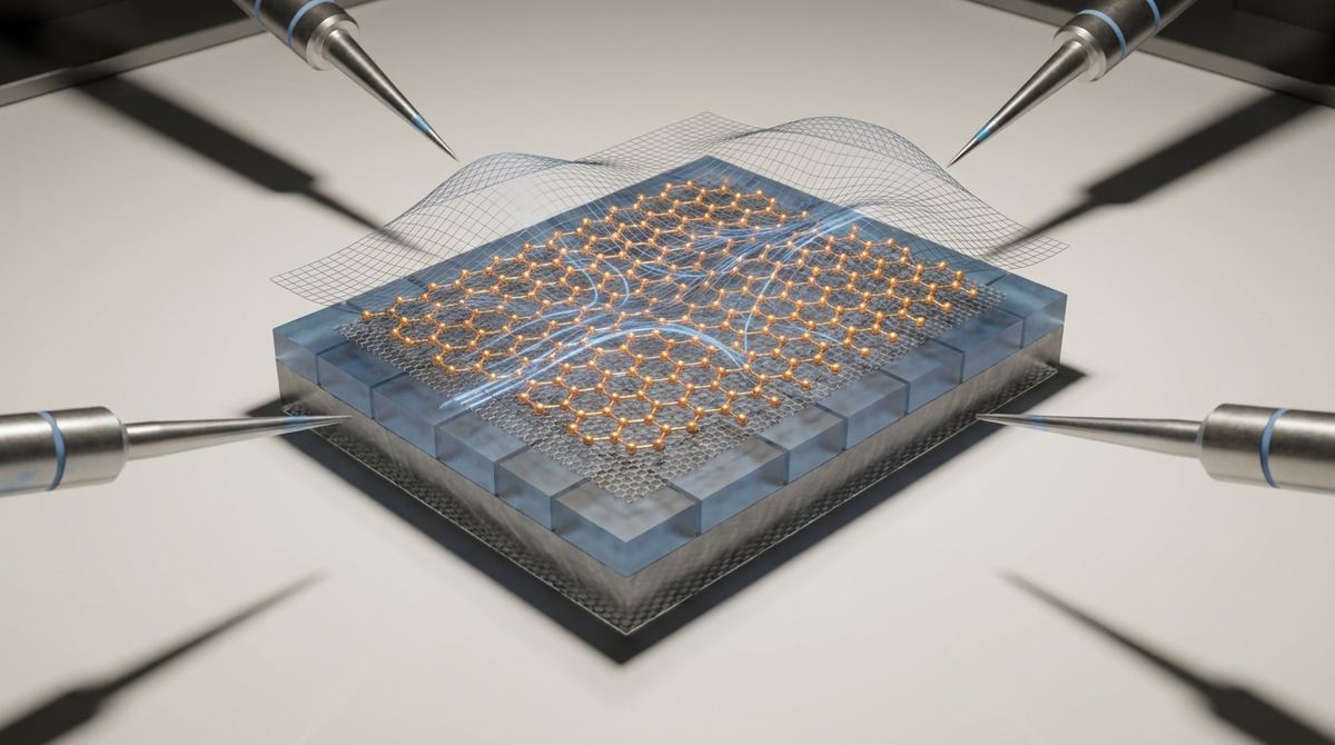
In the quest to build the next generation of supercomputers, scientists are looking far beyond the traditional silicon chips that power our current smartphones and laptops. We are entering an era where the very way we move information through a circuit might change, moving from the simple movement of electrical charge to the sophisticated manipulation of electron spin. At the heart of this revolution is the discovery and manipulation of two-dimensional materials, and a recent breakthrough in the growth of bismuth-based structures is providing a roadmap for this transition. This critical advancement in material science was achieved by a team of researchers including Giorgia Sementilli, Arslan Masood, Fabio Ronci, Stefano Colonna, Marilena Carbone, Marco Papagno, Ziya S. Aliev, Evgueni V. Chulkov, Sergey V. Eremeev, and Roberto Flammini. Their work focuses on a specific, highly ordered arrangement of bismuth known as beta-bismuthene, grown upon a specialized substrate, a feat that could unlock the door to nearly lossless electronic conduction.
As microchips become smaller and more densely packed, they face a fundamental physical barrier known as the heat wall. In traditional silicon-based transistors, electricity moves by shifting charge through a semiconductor. This process inevitably encounters resistance, which causes electrons to collide with the atomic lattice of the material. These collisions generate heat, which limits how fast a processor can run before it melts or requires massive cooling systems. Furthermore, as we approach the atomic scale, the classical laws of physics that govern silicon start to break down due to quantum interference, making it harder to control the flow of electricity.
To overcome these limits, engineers need materials that can conduct information with minimal energy loss and higher precision. This requires moving away from bulk materials toward two-dimensional systems, where electrons are confined to a single plane. However, a major hurdle in 2D materials science is the interface. When you place one layer of material on top of another, they often do not "talk" to each other correctly. The atoms might not line up, creating defects and cracks that scatter electrons and ruin the material's potential. The research presented here aims to solve this specific engineering problem: how to grow a perfect, high-quality layer of a 2D material on a specific substrate so that the two materials work in perfect harmony rather than fighting against each other.
To understand this research, imagine you are trying to lay a sheet of highly patterned, decorative glass over a surface made of moving water. If you just drop the glass on the water, it will tilt, crack, or sit unevenly. But if the water were frozen into a perfectly structured, repeating pattern of ice, you could lay the glass so that every ridge on the glass fits perfectly into every valley in the ice. This process of growing a new crystal layer that follows the exact pattern of the layer beneath it is called epitaxy.
In this study, the researchers are not using water and glass, but atoms and crystalline surfaces. They are using a "template" material called Sb2Te3 (antimony telluride) to guide the bismuth atoms into a very specific shape called beta-bismuthene. Instead of bismuth forming a random, chunky mass, the underlying pattern of the antimony telluride forces the bismuth atoms to arrange themselves into a beautiful, flat, two-dimensional sheet. This specific shape, the beta-phase, is essential because it possesses the unique electronic properties required for next-generation electronics, such as the ability to move electrons with almost no resistance.
The material being studied, bismuthene, is often referred to as the bismuth analog to graphene. While graphene is a single layer of carbon atoms, bismuthene is a single layer of bismuth atoms. Bismuth is a very heavy element, which gives it a property called strong spin-orbit coupling. This is a quantum mechanical effect where the electron's spin (its internal magnetic orientation) is tightly linked to its orbital motion (the path it takes through the material). This link is the engine behind spintronics, a field that aims to use the spin of an electron, rather than just its charge, to store and process data.
The reason this system is so complex involves the interaction between the bismuthene and the Sb2Te3 substrate. Sb2Te3 is a topological insulator. These are strange materials that act as insulators in their bulk interior but have highly conductive, protected pathways on their surfaces. When the beta-bismuthene is grown epitaxially on this substrate, the electronic clouds of the bismuth atoms overlap with the electronic clouds of the antimony and tellurium atoms.
This overlap is not accidental; it is a controlled interaction. The structure of the Sb2Te3 provides a lattice—a repeating geometric grid—that matches the requirements of the beta-bismuthene. Because the lattice of the substrate and the new bismuthene layer are synchronized, the electrons can move across the interface without being scattered by structural mismatches. This synchronization is what allows the unique "topological" properties of the substrate to influence the bismuthene, creating a hybrid system where electrons can travel in one direction without ever hitting an obstacle.
The researchers successfully demonstrated the epitaxial growth of the beta-phase of bismuthene on the Sb2Te3 substrate. This is a significant technical achievement because the beta-phase is a specific, highly stable electronic configuration that does not naturally occur in bulk bismuth. By using the Sb2Te3 as a template, the team managed to force the bismuth atoms into this high-performance 2D state.
The study confirmed that the resulting bismuthene layer was not just a random coating, but a highly ordered, single-crystal-like layer that adhered to the symmetry of the underlying substrate. This structural perfection is vital. The researchers found that the interface between the bismuthene and the antimony telluride was clean and well-defined, meaning the electronic properties of both materials could potentially be leveraged together. This success proves that we can use topological insulators as structural templates to create new, hybrid 2D materials that do not exist in nature, specifically tailored for high-speed, low-energy electrical transport.
The implications of this research are profound for the field of condensed matter physics and materials engineering. By proving that beta-bismuthene can be grown on Sb2Te3, the researchers have provided a blueprint for creating "heterostructures"—stacked layers of different materials that possess combined properties.
The primary value lies in the reduction of energy dissipation. Because the beta-bismuthene can support protected electronic states, electrons can move through the material with much less resistance than they would in a silicon-based component. This could lead to processors that generate significantly less heat, allowing for much higher clock speeds and higher density in microchips.
Furthermore, this research advances the field of spintronics. In traditional electronics, we fight against the magnetic noise and heat caused by moving charge. In a spintronic device enabled by these bismuthene-topological insulator hybrids, we could control the "spin" of the electron to represent 0s and 1s. Since spinning an electron requires much less energy than moving its charge through a resistive wire, this could lead to a massive leap in energy efficiency for data centers and mobile devices.
While this is a major scientific milestone, it is important to recognize that this research is currently in the fundamental laboratory stage. The growth of these materials typically requires highly controlled environments, such as ultra-high vacuum chambers and specialized deposition equipment, which are not currently used in standard mass-production chip factories.
Scaling this process is the next great challenge. While we can grow a small, perfect flake of bismuthene in a lab, growing a large, continuous sheet of it across a 12-inch silicon wafer without a single defect is an entirely different engineering feat. Additionally, the stability of these 2D layers is a concern. Many 2D materials are sensitive to air, moisture, and temperature fluctuations, which can cause them to degrade or lose their unique electronic properties. Future research will need to focus on "encapsulation" techniques to protect these thin films and studies on how these materials behave under the high-temperature processes used in commercial semiconductor manufacturing.
The path from the lab to the consumer market involves several key industries. The first is the semiconductor industry, where the goal is to replace or augment silicon with 2D heterostructures to drive the next generation of computing. This includes everything from higher-frequency processors for artificial intelligence to more efficient memory storage modules.
Another critical application is quantum computing. Quantum bits, or qubits, are extremely fragile and prone to "decoherence," where they lose their quantum information due to interaction with the environment. The protected electronic states found in topological insulators and 2D bismuthene could provide a more stable environment for qubits, helping to shield them from the noise that currently plagues quantum systems.
Finally, the field of sensing and metrology will benefit. The extreme sensitivity of 2D electron gases to external electrical and magnetic fields makes them perfect for highly precise sensors used in medical imaging, autonomous vehicle navigation, and advanced scientific instrumentation.
If you remember only one thing from this research, let it be this: scientists have successfully used the atomic pattern of a topological insulator to "mold" bismuth into a highly efficient, two-dimensional sheet, providing a new way to build incredibly fast and energy-efficient electronic devices.
Question: What is bismuthene and why is it special?
Answer: Bismuthene is a two-dimensional version of bismuth, where the atoms are arranged in a single, flat layer. It is special because it possesses strong spin-orbit coupling, a quantum property that allows for much more efficient control of electron spin than traditional materials like silicon.
Question: What does "epitaxial growth" actually mean?
Answer: Epitaxial growth is a method used in crystal manufacturing where a new layer of atoms is grown on a solid surface in a way that follows the exact structural pattern of that surface. It is like using a mold to ensure that the new material fits perfectly on top of the old one.
Question: Why can't we just use silicon for everything?
Answer: Silicon is the current standard, but it is reaching its physical limits. As it gets smaller, it generates too much heat and becomes difficult to control due to quantum effects. We need new materials like bismuthene to continue making computers faster and more efficient.
Question: What is a topological insulator?
Answer: A topological insulator is a unique material that acts like an insulator on the inside (blocking electricity) but acts like a highly efficient conductor on its surface. This unique duality allows for the movement of electrons without much resistance.
Question: Is this technology going to be in my next phone?
Answer: It is unlikely in the immediate future. This research is currently in the fundamental discovery phase. Before these materials appear in consumer electronics, scientists must figure out how to grow them at a large scale and protect them from environmental damage.
The work conducted by Sementilli, Masood, and the entire research team marks a significant step forward in our ability to engineer matter at the atomic scale. By mastering the epitaxial growth of beta-bismuthene on Sb2Te3, they have demonstrated that we can create complex, hybrid quantum materials that bridge the gap between fundamental physics and practical engineering. As we move toward an era defined by quantum computing and ultra-low-power spintronics, these 2D heterostructures will likely serve as the foundation for the next great leap in computational power.
Serious about B2B integration? Test our premium Pulsed Electrical Resistive Carbon Heating turbostratic graphene in your lab. 100g sample packs available now.
Explore More
Researchers reveal how breaking inversion symmetry in 2D metals enables electronic Raman scattering, a powerful, non-destructive tool for characterizing...

Researchers use AI to accelerate the discovery of new materials, identifying a graphene-boron nitride composite for interstellar spacecraft shielding.

In BN-encapsulated graphene, the ultimate limit on electron speed is not graphene itself, but remote phonon scattering from the insulating layers that...