Introduction to Coherent Perfect Absorption
In standard material science, absorption is typically viewed as a passive process where a material simply converts incident electromagnetic energy into heat. However, a more advanced phenomenon known as Coherent Perfect Absorption (CPA) allows for the total elimination of reflected and transmitted light through controlled interference. When light hits a specific type of scatterer, the waves can be engineered to interfere destructively in all directions except for the absorption path, effectively making the object "invisible" to the reflected signal while capturing all the energy.
The recent research by Ghorashi, Alhulaymi, and Stone (2026) provides a mathematical framework for achieving this in the terahertz (THz) spectrum. They have derived the exact surface conductivity required for coated subwavelength-scale scatterers to achieve CPA. The breakthrough is that this required conductivity can be precisely tuned using graphene. For engineers working in THz sensing, stealth technology, or signal management, this offers a pathway to create devices that can switch between being reflective and being perfectly absorbing by simply applying a voltage to a graphene layer.
The Engineering Application: Tunable THz Signal Absorbers
The most immediate practical application for this research is in the development of tunable THz signal management components. In high-frequency communication or security scanning, managing reflections is critical. A device based on this research would act as a "smart" absorber. By adjusting the chemical potential of the graphene coating, an engineer can tune the device to absorb a specific frequency or angular momentum of THz waves, effectively acting as a frequency-selective, perfect absorber.
This is particularly useful for:
1. THz imaging: Reducing unwanted reflections that cause ghosting in high-resolution scans.
2. Signal Isolation: Creating high-performance isolators in THz circuits.
3. Stealth/Camouflage: Developing surfaces that can be tuned to absorb specific radar-like THz frequencies.
What to Build: A Graphene-Coated Micro-Sphere Array
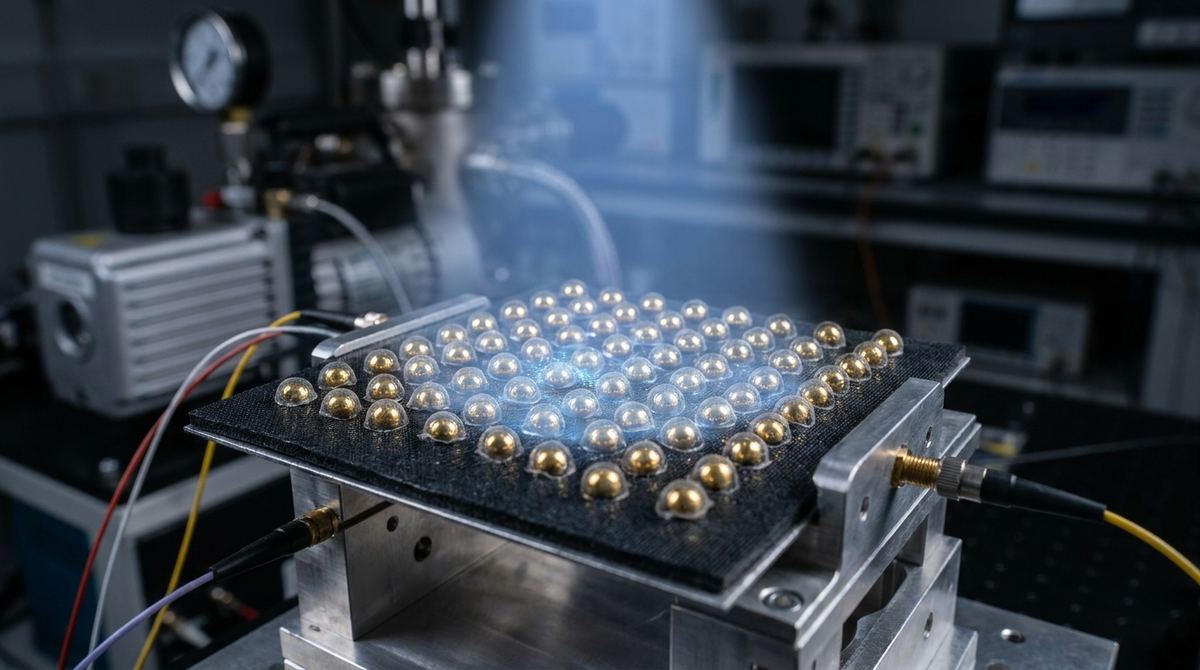
To prototype this effect, the most accessible geometry is an array of coated micro-spheres placed above a conducting substrate. This setup mimics the physics described in the research, where the proximity of a conducting surface allows for the necessary interference to achieve CPA.
Required Materials
Because the research focuses on the terahertz range, the dimensions of your scatterers must be subwavelength relative to the THz wavelength (which ranges from 300 micrometers down to 30 micrometers).
1. Scatterers: Monodisperse silica or gold micro-spheres. For a 1 THz application, spheres with a diameter of 20 to 50 micrometers are recommended.
2. Coating Material: Monolayer CVD graphene. This is essential for the tunable conductivity required by the Ghorashi model.
3. Substrate: A highly conductive surface, such as a gold-coated silicon wafer or a thick copper plate.
4. Tuning Mechanism: An electrochemical gating setup. This requires an electrolyte (such as an ionic liquid) and a gate electrode to allow for the modulation of graphene's carrier density.
5. Deposition Equipment: A spin-coater or a controlled sedimentation setup for arranging the spheres.
6. Transfer Equipment: PMMA-based graphene transfer tools for coating the spheres.
Prototype Assembly Steps
Building this prototype requires precision at the micro-scale.
1. Substrate Preparation: Clean a gold-coated silicon wafer using standard RCA cleaning procedures to ensure a perfectly smooth conducting surface.
2. Scatterer Deposition: Use a controlled sedimentation method to create a periodic array of micro-spheres on the substrate. The spheres should be spaced such that they are dipole-coupled, as suggested by the research for array-based geometries.
3. Graphene Coating: This is the most difficult step. You must transfer a monolayer of CVD graphene onto the spheres. This typically involves using a PMMA support layer, transferring the graphene onto the sphere array, and then using a controlled solvent bath to dissolve the PMMA, leaving the graphene wrapped around the spheres.
4. Electrolyte Application: Apply a thin layer of ionic liquid over the coated spheres. This will act as the medium for the electrochemical gate.
5. Electrical Connection: Attach micro-probes to the graphene layer and the gold substrate to allow for the application of a tuning voltage.
Test and Validation Plan
To verify that your device is achieving Coherent Perfect Absorption, you must perform Terahertz Time-Domain Spectroscopy (THz-TDS).
1. Baseline Measurement: Measure the reflection and transmission of the un-coated sphere array to establish a baseline.
2. Conductivity Tuning: Apply a variable DC voltage through the electrochemical gate. As the voltage changes, the graphene's conductivity changes.
3. Absorption Mapping: Monitor the reflected THz signal. According to the research, there should be a specific voltage (corresponding to a specific conductivity) where the reflected signal drops to near zero.
4. Bandwidth Analysis: Test the device across a range of frequencies (e.g., 0.5 THz to 3.0 THz) to determine the operational bandwidth of your absorber.
5. Angular Momentum Check: If your setup allows for structured light (e.g., using a spatial light modulator), verify that the absorption is optimized for the specific angular momentum state predicted by the Ghorashi model.
Engineering Assumptions and Missing Data
It is important to distinguish between the theoretical findings in the research and the practical engineering assumptions made for this guide.
The research provides the closed-form solution for the required surface conductivity. However, it does not provide specific manufacturing tolerances for the sphere diameters or the exact electrolyte concentration required for stable tuning.
For this guide, we have made the following assumptions:
1. Sphere Size: We assume a diameter of 20-50 micrometers. In a real lab setting, you must calculate the exact diameter based on your target THz frequency to ensure the scatterer remains subwavelength.
2. Doping Method: The research mentions that moderately doped graphene is sufficient. We assume electrochemical gating is the most practical method for a lab prototype, though chemical doping could be used for a permanent, non-tunable version.
3. Geometry: While the research discusses both spheres and cylinders, we assume a sphere-on-conductor geometry for the prototype as it is significantly easier to manufacture via standard micro-fabrication techniques.
Risks and Challenges
1. Graphene Uniformity: The most significant risk is the quality of the graphene transfer. Any cracks, wrinkles, or holes in the graphene layer will cause local variations in conductivity, preventing true perfect absorption and leading to significant scattering.
2. Sphere Monodispersity: If the spheres are not of a uniform size, the resonance condition will vary across the array, making it impossible to achieve a single, sharp absorption peak.
3. Electrolyte Stability: Using ionic liquids for electrochemical gating can be messy and may lead to degradation of the graphene layer over time if the voltage is too high.
4. Impedance Mismatch: Even with perfect conductivity, the transition from the air to the scatterer can cause unwanted reflections. The design must be carefully optimized to ensure the incident wave is correctly coupled to the scatterer.