Imagine a device so thin that it consists of only a single layer of atoms. Such a material is incredibly delicate; even a single stray molecule from the air or a slight irregularity in the surface it sits upon can completely change how it conducts electricity. This sensitivity is both the greatest strength and the most significant weakness of two-dimensional materials like graphene. To harness their true potential, scientists must wrap them in a protective shield, a process known as encapsulation. However, designing these shields is not as simple as putting a material in a box. The very act of wrapping the material changes the quantum mechanical environment, altering the movement of electrons and the fundamental properties of the device. To master this, we need more than just experimental guesswork; we need precise mathematical blueprints that can predict how these encapsulated systems will behave before we ever enter the laboratory.
The Problem This Research Is Solving
The primary obstacle in the field of two-dimensional electronics is environmental interference. When a material like graphene or molybdenum disulfide is exposed to the atmosphere, it interacts with water molecules, oxygen, and the substrate it is resting on. These interactions create what physicists call charge puddles, which are localized areas of varying electrical potential that scatter electrons as they move. This scattering increases resistance and decreases the speed at which a transistor can operate. Encapsulation, typically using a material like hexagonal boron nitride, solves this by providing a pristine, chemically inert environment.
However, this solution introduces a new, complex problem: the interface problem. When you sandwich a 2D material between two layers of an encapsulant, you create a complex three-dimensional system that is actually being driven by two-dimensional physics. The electronic properties of the central layer are no longer determined solely by its own atoms, but by the combined electrostatic influence of the surrounding layers. Standard computational methods often struggle to balance accuracy with efficiency in these scenarios. If a simulation is too simple, it misses the subtle quantum effects that define the material's performance. If the simulation is too complex, it becomes computationally impossible to run, even on the world's most powerful supercomputers. Researchers have struggled to develop a mathematical framework that accurately captures the interaction between the 2D layer and its 3D surroundings without requiring an infinite amount of processing time.
The Key Idea in Plain English
To solve this, researchers turn to a specialized branch of mathematical physics that uses a concept called Kohn-Sham models. In the realm of quantum mechanics, calculating the behavior of every single electron in a piece of material is an impossible task because electrons are constantly interacting with one another in a chaotic dance. The Kohn-Sham approach provides a brilliant shortcut. Instead of tracking every single electron, it simulates a system of non-interacting particles that move in an effective potential. This effective potential is a mathematical construct that accounts for the influence of all the other electrons.
By using these models, scientists can treat the complex many-body problem as a much simpler single-particle problem. This allows us to calculate the electron density of the material with incredible precision. In the context of encapsulated materials, the goal is to refine these mathematical models so they can accurately account for the way the encapsulating layers change the effective potential experienced by the 2D material. This allows engineers to predict how much current will flow through a device or how stable its electronic gap will be, all within a digital simulation.
How the Graphene-Based System Works
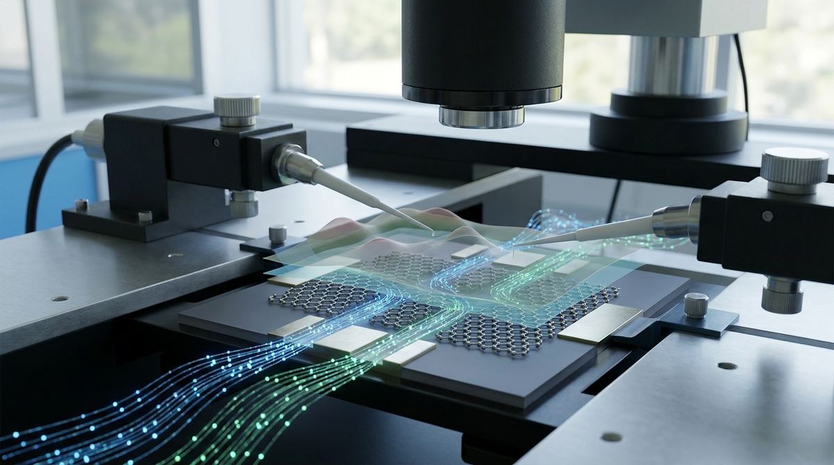
A typical encapsulated system is a microscopic sandwich. At the center is the functional two-dimensional material, which could be graphene for high-speed conduction or a transition metal dichalcogenide for semiconductor applications. Surrounding this core is the encapsulant, most commonly hexagonal boron nitride. This material is ideal because its atomic structure is very similar to graphene, meaning they fit together neatly without creating massive structural defects, and it is an excellent insulator, which prevents unwanted electrical leakage.
When these layers are stacked, the electrons in the central layer experience a specialized electrostatic environment. The presence of the encapsulant provides dielectric screening, which is a phenomenon where the surrounding material helps to dampen the electrical forces between electrons. This screening is crucial because it reduces the intensity of electron-electron repulsions, allowing electrons to move more smoothly and predictably. The Kohn-Sham models used in this research must account for this screening effect with extreme mathematical rigor. They must calculate how the electron density of the 2D layer responds to the presence of the atomic lattices above and below it. This interaction determines the carrier mobility, which is a measure of how quickly an electron can move through the material when a voltage is applied. If the mathematical model correctly predicts this mobility, it provides a reliable blueprint for building faster, more efficient electronic components.
What the Researchers Found
In this mathematical study, Éric Cancès, David Gontier, and Solal Perrin-Roussel focused on the fundamental mathematical foundations required to make these simulations work. Their work belongs to the field of mathematical physics, which means they are not building a physical chip, but rather proving that the mathematical tools we use to design those chips are robust and accurate. They investigated the properties of Kohn-Sham models specifically applied to these layered, encapsulated geometries.
The researchers addressed the complexities that arise when you move from a purely two-dimensional mathematical model to one that accounts for a three-dimensional environment. Their work helps establish the conditions under which these models provide stable and unique solutions for the electron density. By refining the mathematical framework, they provide the theoretical justification needed for other scientists to use these models in practical engineering. This ensures that when a simulation predicts a certain level of conductivity or a specific electronic bandgap for an encapsulated material, that prediction is grounded in rigorous mathematical proofs rather than just being an approximation that might fail in real-world conditions.
Why the Result Matters
The implications of this mathematical refinement are profound for the future of semiconductor technology. As the electronics industry reaches the limits of traditional silicon technology, the race is on to find new materials that can continue to scale down. Two-dimensional materials are the frontrunners, but they cannot be used reliably until we can simulate them with absolute certainty. The work by Cancès, Gontier, and Perrin-Roussel provides the necessary confidence in the computational tools used by materials scientists.
When we can accurately model encapsulated materials, we reduce the immense cost and time associated with "trial and error" engineering. In the past, an engineer might spend months synthesizing a new material stack in a lab, only to find that its electrical properties were not what was expected due to unforeseen interface effects. With the mathematical frameworks provided by this research, engineers can perform high-fidelity simulations to test thousands of different material combinations virtually. This accelerates the transition from a laboratory curiosity to a commercially viable component in a smartphone, a quantum computer, or a high-performance sensor.
Limitations and What Still Needs Testing
While this research provides a vital mathematical foundation, it is important to distinguish these theoretical models from physical reality. The models discussed are mathematical abstractions that assume a level of perfection that is difficult to achieve in a manufacturing plant. For instance, the models may assume a perfectly clean interface between the graphene and the boron nitride, whereas in a real factory, there might be microscopic wrinkles, dislocations, or trapped impurities that the current mathematical models do not yet fully capture.
Furthermore, while these models are highly effective for understanding the electronic structure, they are computationally intensive. Even with the refinements provided by this research, simulating large-scale devices—such as a complex circuit containing millions of transistors—remains beyond our current computational reach. Most current work focuses on a single layer or a single junction. To reach full industrial implementation, these mathematical models must be scaled up to handle more complex, non-idealized environments and more complex device architectures.
Real-World Applications
The ability to model and eventually manufacture encapsulated 2D materials opens doors to several transformative technologies. In the field of high-frequency electronics, graphene-based transistors could operate at speeds far exceeding current silicon-based technology, enabling faster communication networks and more efficient power management in consumer electronics. Because the encapsulation protects the graphene, these devices would be more stable over time, making them suitable for long-term industrial use.
In the emerging field of quantum computing, 2D materials are being explored for use in creating qubits. Quantum states are incredibly fragile and can be destroyed by the slightest bit of environmental noise. Encapsulated 2D materials offer a way to create a "quiet" environment for quantum bits, and the mathematical models developed by researchers like Cancès, Gontier, and Perrin-Roussel allow scientists to design these quantum environments with unprecedented precision. Additionally, ultra-sensitive sensors for detecting biological molecules or chemical changes in the environment could benefit from the high signal-to-noise ratio provided by encapsulated 2D layers, as the protection prevents the sensor from being "blinded" by environmental interference.
If You Remember One Thing
If there is one takeaway from this research, it is that the future of ultra-fast, miniature electronics depends as much on advanced mathematics as it does on the materials themselves; without rigorous models to guide us through the complex quantum interactions of encapsulated layers, we cannot reliably engineer the next generation of technology.
FAQ
What is the purpose of encapsulation in two-dimensional materials?
Encapsulation is the process of sandwiching a thin material, like graphene, between two layers of a protective substance such as hexagonal boron nitride. This is done to shield the sensitive 2D material from environmental contaminants like oxygen or water and to minimize electrical noise from the substrate, which allows the material to perform at its maximum theoretical efficiency.
Why are Kohn-Sham models used in materials science?
Kohn-Sham models are a mathematical way to simplify the incredibly complex problem of how thousands of electrons interact with each other. Instead of calculating every single interaction, the model uses an effective potential to simulate how electrons move, making it possible for computers to accurately predict the properties of new materials.
How does this research help engineers building new electronics?
By providing mathematically proven models for encapsulated materials, this research gives engineers a reliable way to simulate how a device will behave before they actually build it. This reduces the need for expensive and time-consuming laboratory testing and helps prevent failures caused by unexpected quantum effects at the material interfaces.
Is this research related to making new materials in a lab?
This specific research is focused on the mathematical physics and the theoretical models used to understand materials, rather than the physical creation of materials in a laboratory. It provides the "rules" and the "blueprints" that lab scientists and engineers use to ensure their physical experiments are successful and predictable.
What are the limits of using simulations instead of physical testing?
While simulations are incredibly powerful, they are only as good as the math and the assumptions behind them. A simulation might assume a perfect, defect-free material, but in a real-world manufacturing process, there may be tiny scratches, wrinkles, or chemical impurities that the simulation did not account for, meaning physical testing is always necessary to confirm results.
Conclusion
The journey toward a new era of electronics requires us to master the delicate physics of the atomic scale. The research conducted by Éric Cancès, David Gontier, and Solal Perrin-Roussel provides a critical bridge between abstract mathematical theory and practical engineering. By refining the Kohn-Sham models used to simulate encapsulated two-dimensional materials, they have helped build the foundation upon which the next generation of high-speed, stable, and incredibly small electronic devices will be constructed. As we move from the theoretical perfection of math to the messy reality of manufacturing, these rigorous models will be the guiding light for the engineers of tomorrow.