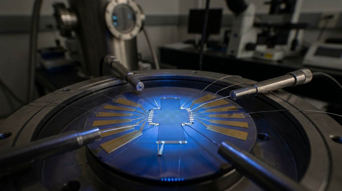
Overview of the Application
The ability to detect magnetic flux at the single-vortex level is a holy grail for quantum computing and ultra-sensitive magnetometry. Recent research by Perego et al. has demonstrated that magic-angle twisted bilayer graphene (MATBG) can be used to create gate-defined Josephson junctions (JJ) capable of sensing individual magnetic vortices.
For an engineering team or a specialized lab, this presents a pathway to building a new class of quantum-limited sensors. Unlike traditional SQUIDs (Superconducting Quantum Interference Devices) that measure bulk magnetic fields, a graphene-based JJ sensor can detect the discrete movement of vortices through the superconducting leads. This is achieved by monitoring shifts in the Fraunhofer interference pattern of the critical current and analyzing voltage noise. This guide outlines how to prototype a device capable of observing the transition from thermal vortex creep to macroscopic quantum tunneling.
The Core Concept
In a magic-angle twisted bilayer graphene device, the electronic properties are highly sensitive to the twist angle, which must be approximately 1.1 degrees. When tuned to this angle, the material becomes superconducting. By using a local gate electrode, you can create a narrow region where superconductivity is suppressed, effectively forming a Josephson junction.
When a magnetic field is applied, magnetic flux enters the superconducting leads in the form of quantized vortices. As these vortices move or fluctuate, they disrupt the phase coherence across the junction. This disruption manifests in two measurable ways:
1. A shift in the critical current (Ic) as a function of the magnetic field (B), known as the Fraunhofer pattern.
2. Telegraph-type noise in the voltage (V) traces, caused by rapid vortex fluctuations.
By monitoring these signals, you can detect not just the presence of a field, but the actual quantum-mechanical behavior of the vortices themselves.
Required Materials and Equipment
Building this device requires advanced nanofabrication capabilities and specialized cryogenic equipment.
Materials:
1. High-quality hexagonal Boron Nitride (hBN) flakes for encapsulation.
2. Monolayer graphene flakes.
3. Silicon/Silicon Dioxide (Si/SiO2) substrates.
4. Gold and Chromium for electrical contacts.
5. PMMA or similar resist for electron-beam lithography.
Equipment:
1. A high-resolution Transmission Electron Microscope (TEM) or specialized AFM for angle verification.
2. An Electron-Beam Lithography (EBL) system for gate and contact patterning.
3. A Dilution Refrigerator capable of reaching temperatures below 10 mK.
4. Ultra-low-noise DC and AC voltage sources.
5. High-speed, low-noise digitizers for voltage noise spectroscopy.
Prototype Fabrication Steps
The success of this device depends entirely on the precision of the twist angle and the cleanliness of the graphene-hBN stack.
1. Substrate Preparation: Clean a Si/SiO2 substrate and prepare it for the deposition of the first hBN layer.
2. The Tear-and-Stack Method: This is the industry standard for MATBG. Exfoliate a single sheet of graphene and split it into two flakes using a polymer stamp.
3. Precise Twisting: Stack the two graphene flakes on top of each other. The rotation between the two flakes must be precisely 1.1 degrees. Even a deviation of 0.1 degrees can move the material out of the magic-angle regime.
4. Encapsulation: Sandwich the twisted bilayer graphene between two layers of hBN. This protects the graphene from environmental contaminants and provides a pristine dielectric environment.
5. Gate Electrode Patterning: Use EBL to define a local gate electrode underneath the graphene stack. This gate will be used to tune the junction and create the Josephson barrier.
6. Contact Deposition: Pattern gold/chromium contacts using EBL and thermal evaporation to ensure low-resistance electrical connections to the graphene.
7. Verification: Use Raman spectroscopy or specialized microscopy to confirm the twist angle and the quality of the encapsulation.
Testing and Characterization Plan
Once the device is fabricated and mounted in a dilution refrigerator, follow this testing protocol to validate the sensor performance.
1. Critical Current Mapping: Apply a varying magnetic field (B) and measure the critical current (Ic) of the junction. Plot the Ic(B) curve to observe the Fraunhofer interference pattern. A shift or distortion in this pattern indicates the presence of trapped vortices.
2. Voltage Noise Spectroscopy: Set the device at a voltage near the critical current. Use a high-speed digitizer to record the voltage fluctuations V(t). Look for telegraph-type noise, which indicates individual vortices jumping between pinning sites.
3. Temperature Sweep: Gradually increase the temperature from 10 mK up to 150 mK.
4. Data Analysis:
- At higher temperatures (above 100 mK), analyze the vortex motion as thermally activated creep.
- At lower temperatures (below 80 mK), look for the saturation of the fluctuation rates. This saturation is the signature of macroscopic quantum tunneling (MQT) of the vortices.
Engineering Assumptions and Technical Constraints
Because this is an advanced research-grade device, several assumptions must be made during the design phase:
1. Temperature Range: The research indicates that the transition to quantum tunneling occurs below 80 mK. Therefore, your cryogenic system must reliably reach at least 10 mK to observe the quantum regime clearly.
2. Angle Precision: The magic angle is assumed to be 1.1 degrees. However, in a practical lab setting, you should assume a tolerance of +/- 0.05 degrees. If your fabrication process cannot hit this window, the device will behave as a standard metal or semiconductor rather than a superconductor.
3. Junction Dimensions: The research uses a gate-defined junction. For a prototype, assume a junction width in the range of 50 to 200 nanometers. Smaller junctions increase sensitivity but are much harder to fabricate.
4. Noise Floor: The voltage noise measurements require an extremely low noise floor. We assume the use of cryogenic HEMTs (High-Electron-Mobility Transistors) or similar low-noise amplifiers to prevent the measurement electronics from drowning out the vortex telegraph noise.
Risks and Mitigation
1. Fabrication Sensitivity: The most significant risk is the failure to achieve the magic angle. Mitigation: Implement rigorous Raman spectroscopy checks at every stacking step.
2. Thermal Leakage: At 10 mK, even tiny amounts of electrical noise or thermal conduction from the wiring can raise the sample temperature. Mitigation: Use heavy filtering on all electrical lines and ensure the sample is well-thermalized to the mixing chamber of the dilution refrigerator.
3. Contamination: Any trapped hydrocarbons or residues between the graphene and hBN layers will destroy the superconductivity. Mitigation: Perform all stacking in a high-end cleanroom environment using the dry-transfer method.
4. Vortex Pinning: Unwanted defects in the graphene can act as pinning sites, making it difficult to distinguish between intentional vortex dynamics and random defect-driven noise. Mitigation: Use ultra-high-purity hBN and high-quality exfoliation techniques to minimize defect density.