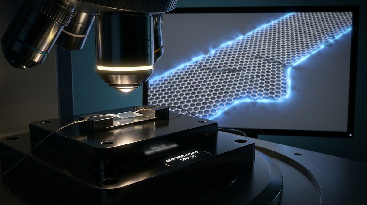
The Challenge of Nano-Scale Interconnects
As semiconductor manufacturing moves toward the sub-5nm regime, traditional copper interconnects face insurmountable resistance and electromigration issues. Graphene nanoribbons (GNRs) offer a potential solution due to their exceptional carrier mobility and ability to maintain electronic properties at extremely small scales. However, a major architectural hurdle remains: how do you connect these one-dimensional wires at an angle to create complex, non-linear circuits?
When two GNRs meet at an angle, the junction often introduces significant scattering or total conductance failure due to the way the carbon lattice is interrupted. For a startup or a research lab attempting to build GNR-based logic gates or routing components, the ability to design a junction that preserves conductance is critical.
Recent research by Leuenberger, Čerņevičs, and Yazyev provides a roadmap for solving this. They demonstrate that we do not need to create perfectly seamless, complex junctions. Instead, we can use a technique called trimming—selectively removing atoms at the junction edge—to create efficient connections. This guide outlines how to prototype a GNR junction testbed using these findings.
The Engineering Principle: The Edge Ratio Model
The core discovery in the research is that the conductance of a GNR junction is not determined by the total area of the junction, but rather by the ratio of armchair edges to zigzag edges at the connection point.
In graphene, armchair edges and zigzag edges have fundamentally different electronic behaviors. Zigzag edges tend to host localized states that can interfere with carrier flow, while armchair edges are often more conducive to maintaining the desired transport properties. The research shows that as long as you trim the junction such that the probability density current at the tip remains negligible, you can remove atoms without a significant drop in conductance.
For an engineer, this means the design goal is no longer about making the junction as smooth as possible. Instead, the goal is to engineer the specific ratio of armchair to zigzag edges at the junction to match the required conductance for your specific circuit.
What to Build: A GNR Junction Testbed
The goal is to build a prototype device that consists of two GNRs meeting at a controlled angle, with a "trimmed" junction area. This testbed will allow you to correlate the physical geometry of the junction (the edge ratio) with the measured electrical conductance.
Materials and Tools
Because this application operates at the atomic scale, standard fabrication tools are required.
1. Substrate: Hexagonal Boron Nitride (hBN) on Silicon/Silicon Dioxide (SiO2/Si). hBN is preferred over SiO2 to minimize substrate scattering and provide an atomically flat surface.
2. Graphene: High-quality, large-area CVD-grown graphene or exfoliated monolayer graphene.
3. Patterning Tool: Electron Beam Lithography (EBL) system. This is essential for the precision required to "trim" edges at the nanometer scale.
4. Etching: Reactive Ion Etching (RIE) with Oxygen plasma for precise edge definition.
5. Metallization: Electron beam evaporator for depositing Ti/Au contacts.
6. Measurement: A cryostat with a 4-point probe setup and a high-sensitivity source measure unit (SMU).
Prototype Fabrication Steps
Since the research is theoretical/computational, the following steps are engineering assumptions for physical implementation. We assume a GNR width of approximately 20nm to 30nm, as this is a standard range for observing quantum confinement effects.
1. Substrate Preparation: Clean the hBN/Si substrate using standard RCA cleaning procedures to ensure no organic contaminants remain.
2. Graphene Deposition: Transfer CVD graphene onto the hBN substrate using a PMMA-assisted transfer method.
3. Primary Patterning: Use EBL to define the main channels of the two GNRs. The angle between the two ribbons should be varied across different test samples (e.g., 30, 45, 60, and 90 degrees) to change the junction geometry.
4. Junction Trimming: This is the critical step. Using a second EBL exposure with a higher dose, define the junction area. The goal is to create a "cut" or "trim" at the intersection. We assume the use of a high-resolution resist like PMMA to achieve the precision required to manipulate the armchair/zigzag ratio.
5. Etching: Perform Oxygen RIE to remove the graphene in the patterned areas, leaving only the GNRs and the specifically trimmed junction.
6. Contact Fabrication: Deposit Ti/Au contacts at the ends of the GNRs. We assume a contact resistance of less than 10k Ohms to ensure the junction properties are the dominant factor in the measurement.
7. Annealing: Perform a vacuum anneal at approximately 250-300 degrees Celsius to improve the contact resistance and remove residual resist.
Test Plan
To validate the design, you must correlate the geometric ratio with the electrical output.
1. Characterization: Use Scanning Electron Microscopy (SEM) or Atomic Force Microscopy (AFM) to verify the junction geometry. While SEM may not resolve individual atoms, it can confirm the angle and the general shape of the trim.
2. Conductance Measurement: Perform I-V (Current-Voltage) sweeps at cryogenic temperatures (e.g., 4K). Low temperatures are necessary to reduce thermal noise and ensure that the transport is in the coherent regime, as suggested by the research.
3. Ratio Correlation: Calculate the ratio of armchair edges to zigzag edges at the junction for each sample. Plot the measured conductance (G) against this ratio (R).
4. Model Verification: Compare your experimental results against the simple model proposed in the Leuenberger et al. paper. If the conductance follows the predicted ratio-based model, the trimming technique is validated for your fabrication process.
Risks and Engineering Assumptions
1. Edge Roughness: The research assumes a controlled trimming of atoms. In practice, RIE and EBL can cause "edge roughness" (jagged edges). If the roughness is too high, the armchair/zigzag ratio becomes unpredictable, and conductance will drop significantly due to scattering.
2. Substrate Interference: We assume hBN provides a perfect substrate. However, any trapped impurities between the graphene and hBN will act as scattering centers, potentially masking the junction's effects.
3. Fabrication Precision: The research is based on atomic-scale manipulation. We assume that current EBL technology can achieve the required precision. If the EBL resolution is insufficient, the "trimming" will be too blunt to achieve the specific edge ratios required.
4. Temperature: We assume measurements must be taken at low temperatures (4K) to observe the effects clearly. At room temperature, thermal broadening may obscure the specific conductance changes caused by the edge ratio.
Source Basis
This guide is based on the research findings of Julien Leuenberger, Kristiāns Čerņevičs, and Oleg V. Yazyev (2026). The core technical premise—that junction conductance is dictated by the armchair-to-zigzag edge ratio and that atomic trimming is a viable connection strategy—is derived directly from their investigation into charge carrier flow in trimmed GNR junctions.