
Transonic Flow: A New Era of Graphene Exfoliation
Researchers have developed a method using transonic flow focusing to peel single layers of graphene from graphite, offering a potential path toward high-quality, scalable production.
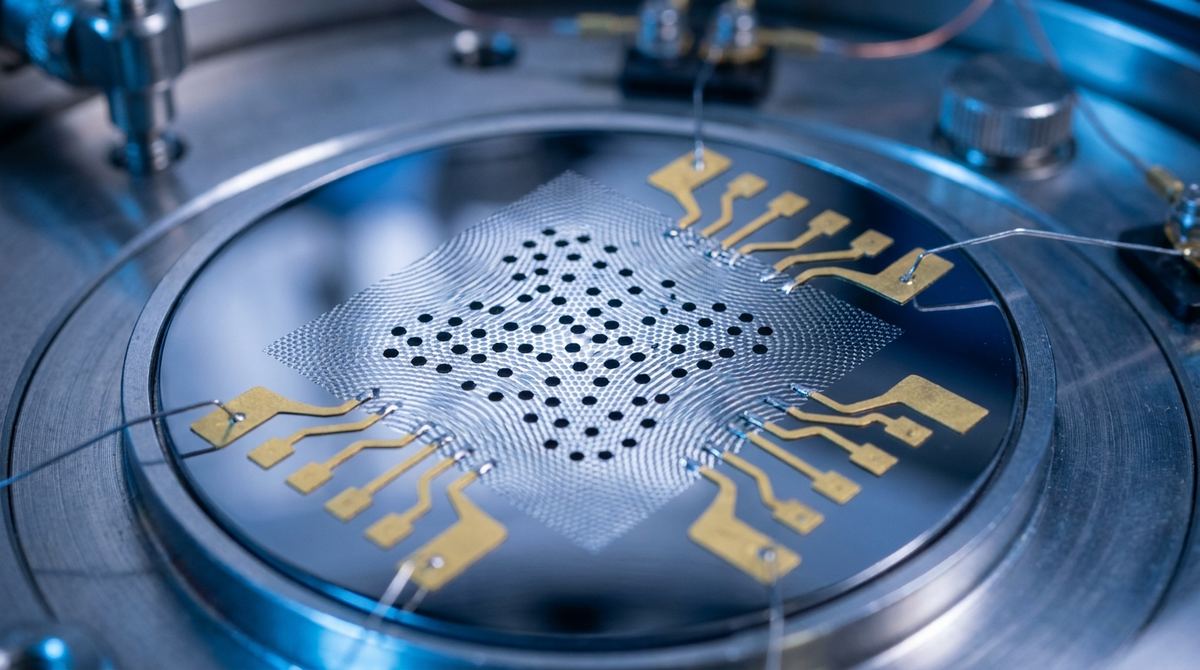
The discovery of fractional Chern insulators (FCIs) in moiré materials has opened a new frontier for quantum hardware development. Unlike traditional quantum Hall effects that require massive magnetic fields, moiré materials like rhombohedral graphene (mRG) allow for the observation of these exotic states through lattice engineering.
A significant challenge for engineers developing quantum sensors or topological qubits is distinguishing between different quantum phases. Recent research has highlighted a critical ambiguity: when a material transitions from an FCI to a different state, is it because the edges of the device are failing to equilibrate, or is the entire bulk of the material undergoing a phase transition?
To solve this, engineers must move away from standard Hall bar geometries and instead develop mesoscopic antidot devices. These devices use nanoscopic holes to probe the bulk properties of the material, effectively bypassing the complications caused by edge state equilibration. This guide outlines the process for prototyping these devices to characterize competing Chern states.
The primary application for this device is in the development of high-precision quantum standards and topological quantum computing components. By successfully characterizing the phase transition from an FCI to a generalized anomalous Hall crystal, engineers can:
1. Validate the stability of fractionalized excitations for use in topological qubits.
2. Develop ultra-precise current standards based on quantized resistance.
3. Map the phase diagrams of moiré materials to optimize material growth for specific quantum states.
While the research provided is fundamental, the engineering implementation is the prerequisite for any commercial startup aiming to utilize moiré-based quantum effects.
Building these devices requires specialized cleanroom capabilities and advanced cryogenic infrastructure.
Materials:
- Moiré rhombohedral graphene (mRG) flakes.
- High-quality hexagonal Boron Nitride (hBN) for encapsulation.
- Gold (Au) for electrical contacts.
- Polyimide or PMMA for resist layers.
- Silicon/Silicon Dioxide (Si/SiO2) substrate.
Equipment:
- Dry transfer station (for hBN/Graphene stacking).
- Electron-beam lithography (EBL) system.
- Reactive Ion Etching (RIE) system (for antidot creation).
- Thermal evaporator or Sputter coater (for metal deposition).
- Dilution refrigerator (capable of reaching temperatures below 150mK).
- Low-noise measurement electronics (Lock-in amplifiers and high-sensitivity pre-amplifiers).
The fabrication of an antidot device is significantly more sensitive than standard graphene transistors due to the requirement of maintaining the moiré twist angle and minimizing strain.
1. Sample Stacking: Using a dry transfer method, stack the mRG flake between two layers of hBN. The hBN must be atomically flat to prevent local strain variations that could destroy the moiré pattern. The stack should be placed on a Si/SiO2 substrate.
2. Patterning the Antidot: Use Electron-beam lithography to define a small, circular hole (the antidot) in the center of the graphene flake. The diameter of the antidot should be small enough to be considered mesoscopic relative to the device dimensions but large enough to allow measurable tunneling currents.
3. Etching: Use Reactive Ion Etching (RIE) with an oxygen plasma to etch the hole through the graphene and the hBN encapsulation. This creates the "antidot" structure. Precise control of etch time is critical to avoid over-etching the surrounding graphene.
4. Contact Deposition: Deposit gold contacts using thermal evaporation. These contacts should be designed to allow for tunneling measurements into the antidot region.
5. Final Encapsulation: If necessary, a final layer of hBN can be deposited to protect the device, though this must be done carefully to avoid damaging the etched antidot edges.
Once the device is fabricated, the testing must be conducted at millikelvin temperatures to observe the competing Chern states.
1. Temperature Sweep: Begin measurements at 4K and slowly decrease the temperature. The target is to observe the transition near 150mK.
2. Bulk Resistance Measurement: Monitor the resistance of the bulk material. According to recent findings, a thermodynamic phase transition from an FCI to an anomalous Hall crystal is expected to occur below approximately 150mK.
3. Tunneling Spectroscopy: Use a mesoscopic probe to measure quasiparticle charging. At specific filling factors, such as nu=1 and nu=2/3, the device should reveal quasiparticles carrying exactly one electron charge.
4. Filling Factor Mapping: Vary the gate voltage to sweep through different filling factors. This allows you to map the stability regions of the fractional Chern insulator states.
Prototyping at this scale involves several high-probability failure modes.
- Strain Management: Any mechanical strain introduced during the stacking process will alter the moiré potential and can shift the phase transition temperature or destroy the FCI state entirely. Mitigation: Use high-precision, temperature-controlled transfer stages and minimize contact pressure.
- Thermal Decoherence: The target physics occurs below 150mK. If the device has high thermal coupling to the substrate or poor electrical shielding, the temperature of the electrons may remain much higher than the mixing chamber temperature. Mitigation: Use high-quality thermal anchoring for all electrical leads and minimize electron heating through low-excitation measurements.
- Surface Contamination: Even a single layer of hydrocarbons from the atmosphere can ruin the electronic properties of the mRG. Mitigation: Perform all fabrication steps in a controlled environment and use vacuum-based etching and deposition.
- Etch Damage: The RIE process can damage the edges of the antidot, creating dangling bonds that lead to charge noise. Mitigation: Optimize plasma power and pressure to achieve a "soft" etch that preserves the crystalline integrity of the graphene edges.
This guide is based on the research findings published by Li et al. (2026) regarding the transition between competing Chern states in moiré rhombohedral graphene.
The engineering assumptions made in this guide include:
- The assumption that a standard EBL/RIE process is sufficient to create an antidot without destroying the moiré periodicity.
- The assumption that the device can be cooled to 150mK or lower without significant electronic heating.
- The assumption that the transition observed in the research is a bulk thermodynamic transition, which justifies the use of an antidot to probe the bulk rather than the edges.
Engineers should treat the 150mK threshold as a critical design parameter for the cryogenic system and the 150mK transition as the primary benchmark for device success.
Serious about B2B integration? Test our premium Pulsed Electrical Resistive Carbon Heating turbostratic graphene in your lab. 100g sample packs available now.
Explore More
Researchers have developed a method using transonic flow focusing to peel single layers of graphene from graphite, offering a potential path toward high-quality, scalable production.

Discover how Kekulé-Y graphene allows for unprecedented control over light through mechanical strain and electrical doping, paving the way for highly tunable optical devices.

A practical guide for developing prototype topological quantum logic elements using the switchable chiral superconductivity found in rhombohedral hexalayer graphene.