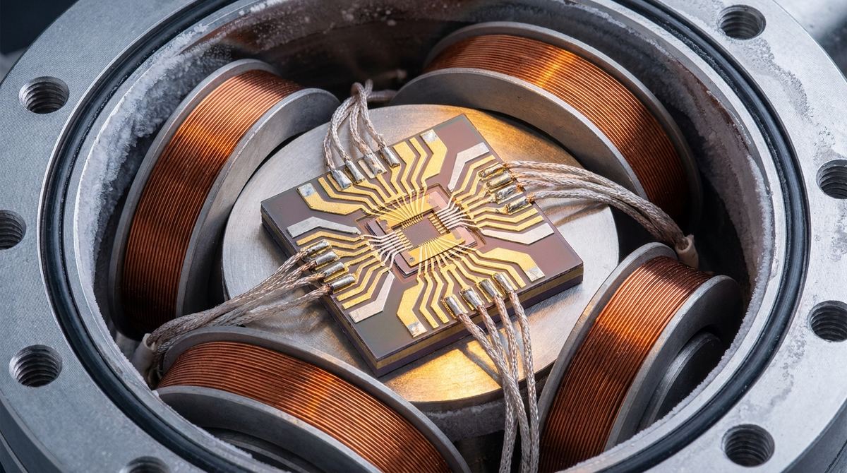
The Engineering Objective: Programmable Topological Logic
The recent discovery of a switchable chiral-superconductor quartet in rhombohedral hexalayer graphene (R6G) provides a new architecture for topological quantum computing components. In traditional superconducting circuits, states are often fixed by the physical geometry of the device. However, R6G introduces a multi-knob control mechanism. By manipulating the out-of-plane magnetic field, the carrier density, and the gate displacement field, an engineer can switch the material between a quarter-metal (QM) state and a superconducting state (SCH).
The practical application for a startup or advanced lab is the creation of a programmable topological switch. When the material transitions between these states, it creates a domain wall. According to the research, these domain walls are expected to host Majorana zero modes—quasiparticles that are their own antiparticles and obey non-Abelian statistics. A device that can move these domain walls by simply adjusting a gate voltage or a magnetic field is essentially a programmable topological logic gate.
Required Materials and Hardware
Building a prototype in this regime requires specialized cryogenic and nanofabrication equipment. You cannot test this at room temperature or even in standard liquid helium environments.
1. Rhombohedral Hexalayer Graphene (R6G) flakes. This is the most critical and difficult component. Unlike monolayer graphene, R6G requires precise stacking of six layers in a specific rhombohedral orientation. This is typically achieved through mechanical exfoliation and high-precision dry transfer techniques.
2. Hexagonal Boron Nitride (hBN). High-quality, ultra-flat hBN is required for encapsulation to protect the R6G from environmental contamination and to provide a clean dielectric environment.
3. Substrate. A silicon substrate with a thick oxide layer (SiO2) or a specialized sapphire substrate can be used, but the substrate must allow for both top-gate and back-gate configurations.
4. Electrodes. Gold (Au) or Titanium/Gold (Ti/Au) for electrical contacts. For superconducting leads, Niobium (Nb) or Aluminum (Al) is recommended to facilitate proximity-effect studies.
5. Cryogenic System. A dilution refrigerator capable of reaching temperatures below 100mK is mandatory. The research suggests the superconducting state emerges at low temperatures, and Majorana mode stability requires mK-range environments.
6. Magnetic Field Source. A superconducting magnet capable of providing a stable, tunable out-of-plane magnetic field (H_perp) between 0.8 T and 2.0 T.
7. Precision Electronics. High-resolution, low-noise voltage sources and current sources for gate tuning and transport measurements.
Prototype Fabrication Workflow
The following steps outline the assembly of a dual-gated R6G device designed to create and move domain walls.
1. Substrate Preparation: Clean a Si/SiO2 substrate using standard RCA cleaning protocols to ensure no organic residues remain.
2. R6G Stacking: Using a high-precision micromanipulator or a specialized transfer station (like a vacuum-based transfer system), stack six layers of graphene. The stacking must be strictly rhombohedral to ensure the specific electronic properties described in the research. This is often done by stacking individual layers of graphene or by using thick graphite flakes and carefully controlling the twist angle.
3. Encapsulation: Sandwich the R6G flake between two layers of hBN. This protects the active region and provides the necessary dielectric environment for the displacement field (D) control.
4. Lithography: Use electron-beam lithography (EBL) to define the contact areas and the gate regions.
5. Electrode Deposition: Perform metal evaporation (Ti/Au) for the source and drain contacts. If you are testing proximity effects, deposit superconducting Nb leads near the R6G edges.
6. Gate Integration: Implement a dual-gate architecture. This involves a back-gate (the Si substrate itself) and a top-gate (a thin layer of hBN with a metal electrode on top). This setup is essential for independently controlling the carrier density (n) and the displacement field (D).
Test Plan and Parameter Mapping
The goal of the test plan is to map the phase space of the R6G flake to identify the exact boundaries where the superconducting state emerges and where the domain walls form.
1. Baseline Characterization: At zero magnetic field, measure the resistance of the flake while sweeping the back-gate voltage. You are looking for the quarter-metal (QM) phase, which should show specific resistance characteristics.
2. Magnetic Field Sweep: Apply an out-of-plane magnetic field (H_perp). Increase the field from 0 T to 2 T in small increments (0.05 T). The research indicates the superconducting state (SCH) should emerge above 0.8 T. Monitor the resistance for a sharp drop, indicating the onset of superconductivity.
3. Multi-Knob Mapping: Once the SCH state is identified, create a 3D map of the resistance across the (n, D, H_perp) parameter space. This is the most time-intensive part of the test. You are looking for the boundaries where the resistance transitions from the QM state to the SCH state.
4. Domain Wall Identification: By applying a gradient in the displacement field (D) across the flake using the dual-gate setup, you can create a region where one side of the flake is in the QM phase and the other is in the SCH phase. The boundary between these two regions is your target domain wall.
5. Majorana Detection (Advanced): To confirm the presence of Majorana modes, perform low-temperature tunneling spectroscopy using a scanning tunneling microscope (STM) tip or a dedicated superconducting lead. Look for a zero-bias conductance peak at the domain wall, which is a signature of Majorana zero modes.
Engineering Assumptions and Risks
It is important to distinguish between the findings in the research and the engineering assumptions required to build a device.
Assumption 1: The research confirms the existence of the SCH state in R6G, but it does not provide a specific recipe for the stacking of the six layers. We assume that a standard dry-transfer method with high-precision rotation control can successfully produce the rhombohedral symmetry.
Assumption 2: The research discusses the existence of the four spin-valley isospin flavors. We assume that by tuning the gate displacement field (D), an engineer can selectively switch between these flavors to create specific domain wall configurations.
Assumption 3: We assume that the Majorana modes, while theoretically predicted for these domain walls, can be detected using standard transport measurements or tunneling spectroscopy in a laboratory setting.
Risk 1: Sample Quality. The electronic properties of R6G are extremely sensitive to the stacking angle and the presence of impurities. Even a 1-degree deviation in the rhombohedral stacking could destroy the chiral superconductivity.
Risk 2: Thermal Noise. The signals associated with Majorana modes are incredibly small. Any thermal leakage from the measurement lines into the dilution refrigerator will mask the signal.
Risk 3: Complexity of Control. Managing three independent variables (n, D, and H_perp) simultaneously requires highly sophisticated software and hardware synchronization to ensure the device remains in the desired phase during measurement.
Source Basis
This guide is based on the research findings presented in: Hua, Z., et al. (2026). Multi-Knob Switchable Chiral Superconductivity Quartet in Rhombohedral Graphene. arXiv:2607.06520v1. The application of these findings to topological logic gates is an engineering interpretation intended for research and development purposes.