
Harnessing Spin: The Breakthrough of NiI2 and Graphene Heterostructures
Discover how the marriage of 2D magnets and graphene is enabling a new era of spintronics by controlling electron spin at the atomic interface.
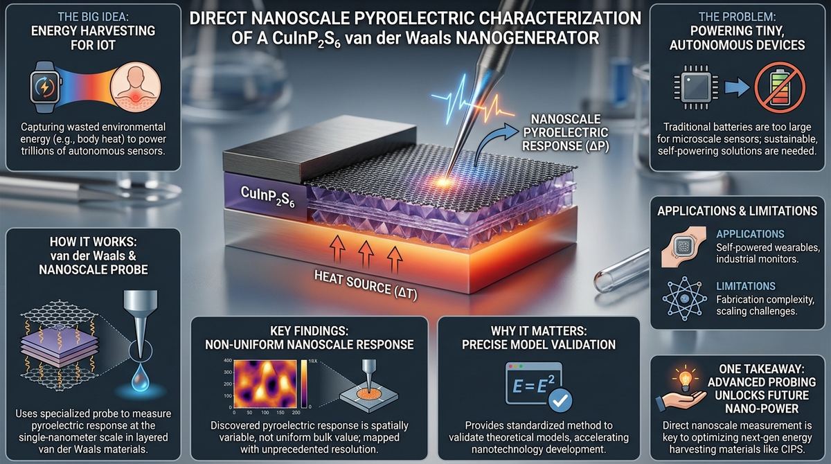
Imagine a world where your smartwatch never needs a charger because it stays powered by the warmth of your skin, or where tiny sensors embedded in industrial engines harvest energy from the heat they produce. This is the promise of energy harvesting, a field dedicated to capturing wasted environmental energy and turning it into electricity. For decades, we have relied on large-scale systems to capture thermal energy, but as our technology shrinks toward the microscopic scale, our methods for capturing this energy must shrink too. The challenge is not just making the device smaller, but understanding how the very physics of energy conversion changes when you are dealing with a single layer of atoms.
As electronic devices become smaller and more integrated, the need for autonomous power sources becomes critical. We are moving toward an era of the Internet of Things, where trillions of tiny sensors will need to function for years without a battery replacement. One of the most abundant sources of energy is heat—ambient temperature fluctuations that occur everywhere from the human body to the surface of a running engine. Pyroelectric materials, which generate an electric charge in response to temperature changes, offer a perfect solution for this.
However, there is a significant technical hurdle in developing these nano-scale power sources. Most of our current understanding of pyroelectricity comes from studying bulk materials, which are large, thick crystals. When you take a material and thin it down to a single layer or a few nanometers of thickness, the physics can change dramatically. Surface effects, interface interactions, and local structural defects start to dominate the behavior of the material. If we only use bulk measurements, we are essentially trying to understand the behavior of a single person by only studying the average behavior of a massive crowd. This lack of precision makes it incredibly difficult for engineers to design reliable, nanoscale energy harvesters. We need a way to look directly at the nanoscale to see how a single flake of material reacts to heat, ensuring that the theoretical models we use to design these devices actually match reality at the atomic scale.
The core concept behind this research is a method of direct, nanoscale measurement. Instead of putting a large chunk of material in a heating oven and measuring the total electricity it produces, the researchers used a specialized probe to interact with the material at a microscopic level. This allows them to pinpoint exactly where and how electricity is generated when the temperature shifts.
Think of it like this: instead of measuring the total amount of water flowing through a massive dam to understand how it works, the researchers are using a tiny, sensitive instrument to measure the movement of a single drop of water as it passes through a narrow channel. By doing this, they can see the subtle details of how the material behaves at its smallest edges and surfaces. This high-resolution approach provides a direct link between the thermal stimulus—the change in temperature—and the electrical output, allowing us to see the true potential of these materials before we try to manufacture them into complex devices.
To understand the system described in this research, we must look at the unique properties of van der Waals materials. While the study focuses on CuInP2S6 (often abbreviated as CIPS), this material belongs to the same fascinating family as graphene. These are two-dimensional materials characterized by strong atomic bonds within a single layer, but very weak forces between the layers. This weak interlayer bonding is known as a van der Waals force, and it allows these materials to be peeled apart into incredibly thin, nearly transparent sheets.
The specific material used here, CuInP2S6, is a non-centrosymmetric crystal. In simpler terms, this means its internal structure is not perfectly symmetrical; the positive and negative charges within the crystal lattice do not perfectly cancel each other out. Because of this asymmetry, the material possesses a property called spontaneous polarization. There is a built-in electrical "imbalance" within the crystal structure.
When the temperature of the material changes, the atoms within the lattice begin to vibrate more or less vigorously. This thermal motion causes the ions to shift their positions slightly. Because the crystal is asymmetrical, this shift in position changes the magnitude of the spontaneous polarization. This change in polarization creates a flow of charge, which we can capture as an electrical signal. In a van der Waals system like this, the thinness of the layers means that the electrical response is incredibly sensitive to the environment. The way the material is placed on a substrate, the presence of any surface defects, and even the way the measurement probe touches the surface can influence the resulting electrical signal. The research focuses on navigating these complexities by using the layered nature of these materials to their advantage, treating each thin flake as a discrete, functional unit of an energy harvester.
In this detailed study, Valentin Fonck, Roop K. Mech, Mohammadali Razeghi, Stuart Finch, Aljoscha Söll, Phillip Dobson, Jonathan R. Weaver, Zdenek Sofer, Oleg Kolosov, Jean Spièce, and Pascal Gehring successfully demonstrated a method for direct nanoscale pyroelectric characterization. By using advanced scanning probe techniques, they were able to map the pyroelectric response of CIPS with unprecedented spatial resolution.
The researchers discovered that the electrical response of the material is not a simple, uniform value as one might expect from bulk measurements. Instead, the characterization revealed that the pyroelectric signal can vary significantly depending on the local environment at the nanoscale. They were able to observe how the thermal stimulus directly translates into electrical activity at the scale of individual material flakes. This was a critical breakthrough because it proved that it is possible to measure these tiny electrical currents without the signal being lost or distorted by the larger environment.
By mapping these responses, the team provided a way to correlate the physical structure of the van der Waals flakes with their electrical performance. This means that if a particular flake is performing poorly, researchers can now look at the nanoscale map to see if the issue is caused by a local defect, a structural mismatch, or the way the material is interacting with the surface it is resting on. This moves the field away from guesswork and toward precise, data-driven engineering of nano-scale energy harvesters.
The implications of this research are profound for the future of nanotechnology. First, it provides a standardized way to validate theoretical models. For years, scientists have used mathematical equations to predict how small a device can be before it stops working efficiently. Now, they have a tool to verify those predictions with real-world, nanoscale data.
Second, this research enables the optimization of material interfaces. In a real-world device, the most important part is often where the material meets the electrical contact. If the contact is poor, the energy generated is lost. By understanding the nanoscale pyroelectric behavior, engineers can design better contact points and more efficient device architectures. This reduces the "lost energy" problem that currently plagues many small-scale electronic designs.
Finally, this work accelerates the development of entirely new classes of sensors. If we can reliably characterize how a single flake of CIPS behaves, we can begin to design sensors that are so small they are essentially invisible, yet capable of operating indefinitely on the ambient heat of their surroundings. This is the foundational science required to move from laboratory curiosity to industrial application.
While this research is a significant leap forward, it is important to recognize that we are still in the early stages of development. The study demonstrates a method for characterization, which is different from creating a mass-producible consumer product. Currently, the techniques used to achieve such high-resolution nanoscale measurements are highly sophisticated, time-consuming, and primarily confined to controlled laboratory settings.
There is also the challenge of material stability. Many 2D van der Waals materials, while possessing incredible properties, can be sensitive to oxygen, moisture, or temperature over long periods. For a device to be useful in a real-world application, like an industrial sensor, it must be able to withstand the environment for years. The research conducted here focuses on the fundamental physics of the material, but more work is needed to understand how these flakes perform under long-term environmental stress. Additionally, the transition from a single, carefully placed flake in a lab to a billion tiny flakes on a silicon chip is a massive engineering challenge that remains to be solved.
The ability to harness energy from heat at the nanoscale opens the door to several revolutionary applications. In the field of medical technology, this could lead to bio-compatible, self-powered implants. An implant that monitors a patient's internal temperature or heart rate could use the body's own heat to power its wireless communication, eliminating the need for dangerous battery replacement surgeries.
In the realm of the Internet of Things (IoT), this research supports the creation of autonomous sensor networks. Imagine thousands of sensors embedded in the concrete of a bridge or the casing of an airplane engine, monitoring structural integrity in real-time. These sensors would require no wiring and no batteries; they would simply live off the thermal fluctuations of the structure itself.
Furthermore, wearable electronics could see a massive boost. Smart clothing that monitors health metrics or tracks athletic performance could be powered by the heat emitted by the wearer's skin. As we master the ability to measure and control these nanoscale electrical responses, the dream of seamless, battery-free electronics will move closer to reality.
If there is one takeaway from this research, it is that the future of energy harvesting lies in our ability to master the physics of the very small. By moving from bulk measurements to direct nanoscale characterization, we are finally gaining the precision needed to turn microscopic heat into meaningful electricity.
What exactly is pyroelectricity?
Pyroelectricity is a physical phenomenon where certain materials generate an electric charge when their temperature changes. This happens because the internal arrangement of atoms in the material shifts when heated or cooled, which changes the material's internal electrical balance and pushes charges toward the surface.
Why is nanoscale measurement so important for these materials?
Most traditional measurement tools are designed for large, bulk samples. However, as we make devices smaller, the way a material behaves changes due to its surface area and the way its layers interact. Nanoscale measurement allows us to see these tiny details, ensuring that our designs for small-scale devices actually work as intended.
What are van der Waals materials?
Van der Waals materials are a special class of materials, like graphene or CuInP2S6, that consist of layers held together by very weak forces. This weakness allows the material to be peeled into incredibly thin sheets, making them perfect for creating ultra-small electronic components.
Can this technology eventually power my smartphone?
While the technology is currently used for research and very small-scale sensing, the goal is to eventually create highly efficient energy harvesters. While it may not power a high-drain device like a smartphone directly anytime soon, it is a crucial step toward creating a world of small, self-powered electronics.
Is CuInP2S6 a better material than graphene for this?
Graphene is excellent for conducting electricity, but it is not pyroelectric, meaning it doesn't produce a charge when heated. CuInP2S6 is specifically chosen for these applications because its crystal structure allows it to convert thermal energy into electricity, making it a functional partner to the conductive properties found in materials like graphene.
The research conducted by Fonck, Mech, Razeghi, and the entire collaborative team marks a pivotal moment in the study of two-dimensional materials. By moving beyond the limitations of bulk measurements and tackling the complexities of nanoscale characterization, they have provided a roadmap for the next generation of energy harvesters. As we bridge the gap between fundamental physics and practical engineering, the ability to capture the energy of a single thermal fluctuation may eventually become the backbone of a new, self-sustaining era of electronics.
END_OF_ARTICLE
Serious about B2B integration? Test our premium Pulsed Electrical Resistive Carbon Heating turbostratic graphene in your lab. 100g sample packs available now.
Explore More
Discover how the marriage of 2D magnets and graphene is enabling a new era of spintronics by controlling electron spin at the atomic interface.

A technical guide for labs and startups to develop topological electronic components by leveraging the twist angle between graphene and WSe2 to switch between Chern insulator and trivial states.

Scientists explore how engineering three-valley moiré patterns in graphene-based materials enables intervalley coherence and flavor polarization, paving the way for advanced quantum information processing.