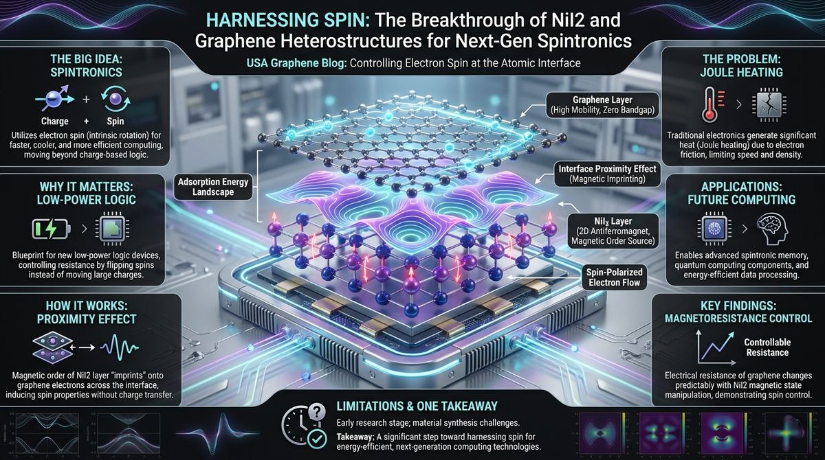
Imagine a computer that does not just process information by moving electrical charges from one place to another, but by manipulating the intrinsic rotation of those electrons, known as spin. In our current technological era, most computing relies on the presence or absence of electrical charge, a process that generates significant heat and limits speed due to the physical resistance encountered by moving electrons. As we reach the physical limits of silicon-based technology, scientists are looking for ways to utilize the spin of the electron to create faster, cooler, and more efficient devices. This frontier is known as spintronics. A recent and profound step in this journey involves the creation of a microscopic sandwich consisting of two distinct two-dimensional materials. By layering nickel iodide, a specialized magnetic material, directly onto a sheet of graphene, researchers have opened a door to controlling electron spin with unprecedented precision. This work, detailed by Stasiu Thomas Chyczewski, Xiaotong Xu, and Wenjuan Zhu, explores the complex physics occurring at the tiny boundary where these two materials meet, a phenomenon that could redefine how we build the hardware of the future.
The Problem This Research Is Solving
The central challenge in modern microelectronics is the heat problem. Every time an electron moves through a traditional semiconductor like silicon, it bumps into atoms, creating friction in the form of heat. This is known as Joule heating. As we try to make processors faster by cramming more transistors into smaller spaces, the heat generated becomes so intense that it threatens to melt the components themselves. This thermal limit is a primary reason why clock speeds in consumer electronics have not increased significantly in recent years.
To solve this, engineers want to move away from charge-based logic and toward spin-based logic. If we can represent a one or a zero using the direction of an electron's spin—up or down—we can potentially perform computations with much less energy. However, there is a massive engineering hurdle: how do you inject a magnetic signal into a non-magnetic conductor like graphene without using bulky, heavy magnets that would destroy the delicate atomic structure of the material?
Furthermore, many existing magnetic materials are three-dimensional, meaning they have significant thickness. When you place a thick magnetic material on top of a thin conductor, the interaction is often messy and inefficient. We need a way to achieve a clean, precise coupling where the magnetic properties of the magnet "leak" into the conductor at the exact point where they touch. This requires working at the atomic scale, where the interface—the junction between the two materials—is the only place where the magic happens. This research seeks to understand exactly how that interface behaves when we pair a specific two-dimensional antiferromagnet with the world's most conductive material, graphene.
The Key Idea in Plain English
The core concept driving this research is known as the proximity effect. Think of it like this: imagine a room filled with people who are all dancing in a very specific, rhythmic pattern. Now, imagine a group of people enters the room, but they aren't dancing to the rhythm yet. However, because they are standing so close to the dancers, they begin to subconsciously pick up the beat, moving their bodies in sync with the original group.
In this analogy, the dancers are the nickel iodide atoms, which have a very strict magnetic order. The people entering the room are the electrons in the graphene. Because the graphene is in direct contact with the nickel iodide, the electrons "feel" the magnetic environment of the nickel atoms. This causes the electrons in the graphene to adopt a specific spin orientation, even though graphene itself is not naturally magnetic.
By using two-dimensional materials, we ensure that every single atom in the graphene is effectively "touching" the magnet. In a bulk, three-dimensional material, most of the atoms are buried deep inside, far away from the surface. In a 2D heterostructure, the interaction is maximized because the surface-to-volume ratio is incredibly high. This allows for a very clean and powerful coupling between the magnetic order and the electrical transport, allowing us to control the movement of electrons by simply turning the magnetism on or off.
How the Graphene-Based System Works
To understand how this system works, we must look at the atomic structures of both components. Graphene is a single layer of carbon atoms arranged in a hexagonal lattice. It is famous for its incredible electrical conductivity, which occurs because its electrons behave like massless particles, moving through the lattice with almost no resistance. However, as mentioned, graphene is not magnetic.
Nickel iodide, or NiI2, is a member of a special class of materials called 2D antiferromagnets. In a ferromagnet, like a standard refrigerator magnet, all the magnetic moments point in the same direction. In an antiferromagnet, the magnetic moments of the atoms point in alternating directions, canceling each other out so that the material has no net external magnetic field. This might sound like it would be useless for spintronics, but it is actually a secret weapon. Because there is no large external magnetic field, these materials do not interfere with each other, allowing us to pack them much more tightly in a microchip without causing magnetic interference or "crosstalk."
When these two materials are layered into a heterostructure, the carbon atoms of the graphene and the nickel atoms of the NiI2 come into close proximity. This proximity allows for the overlap of electronic orbitals. Specifically, the d-orbitals of the nickel atoms interact with the pi-orbitals of the graphene. This interaction creates an "exchange field" at the interface.
This exchange field acts as a subtle but powerful force that splits the energy levels of the electrons in the graphene. Instead of electrons moving freely with the same energy, the spin-up electrons and spin-down electrons now experience different electrical potentials. This is the essence of interfacial magnetotransport. When we pass an electrical current through the graphene, the resistance of that current becomes dependent on the magnetic state of the nickel iodide layer. By applying a magnetic field or changing the temperature, we can flip the magnetic alignment of the NiI2, which in turn changes the electrical resistance of the graphene. We have essentially created a way to translate magnetic information into electrical signals at a single atomic interface.
What the Researchers Found
The research conducted by Stasiu Thomas Chyczewski, Xiaotong Xu, and Wenjuan Zhu focuses on the intricate details of this magnetotransport. The primary finding is that the magnetic order in the NiI2 layer can effectively "imprint" its properties onto the graphene layer through the interface.
The researchers observed that the electrical resistance of the graphene layer changes in a predictable and measurable way when the magnetic state of the NiI2 layer is manipulated. This is a direct observation of the proximity effect in action. Specifically, they were able to detect signatures of the antiferromagnetic order of the NiI2 within the electrical measurements of the graphene. This is a significant technical achievement because antiferromagnets are notoriously difficult to detect and manipulate compared to ferromagnets.
The results demonstrate that the interface is not just a passive boundary but an active participant in the physics of the system. The strength of the magnetotransport signal depends heavily on the quality of the interface. If there are impurities, defects, or gaps between the graphene and the NiI2, the coupling weakens, and the magnetic signal is lost. The study confirms that when a pristine, atomically flat interface is achieved, the exchange interaction is strong enough to influence the electron transport properties of the graphene, providing a clear pathway for creating spintronic devices. This confirms that 2D antiferromagnets are viable candidates for controlling spin in highly conductive 2D electron systems.
Why the Result Matters
This discovery is vital because it provides a blueprint for a new type of "low-power" logic. If we can control the resistance of a material by flipping spins rather than pushing a massive amount of charge through a resistive wire, we can drastically reduce the power consumption of every single operation a computer performs.
The ability to use antiferromagnets like NiI2 is particularly exciting for the scaling of technology. As we move toward a world of massive data centers and billions of connected IoT devices, the energy required to power our digital infrastructure is becoming a global concern. Spintronic devices based on 2D heterostructures offer a way to increase computational density without a corresponding explosion in heat production.
Furthermore, this research bridges the gap between fundamental materials science and practical device engineering. By proving that magnetotransport can be controlled through an interface in these specific 2D systems, the researchers have provided the foundational physics that engineers will need to design actual transistors, memory cells, and sensors. It moves the field of spintronics from a theoretical curiosity into the realm of measurable, controllable, and predictable engineering.
Limitations and What Still Needs Testing
While the results are groundbreaking, it is important to maintain a realistic perspective on how close this is to your smartphone. Currently, the fabrication of these heterostructures typically involves a process called mechanical exfoliation—essentially using specialized adhesive tape to peel layers of material off a crystal. While this is perfect for laboratory research, it is not a scalable manufacturing process. For this technology to reach the mass market, we need to develop methods like Chemical Vapor Deposition (CVD) that can grow these 2D layers over large areas with atomic perfection.
Temperature is another significant hurdle. Many of the most interesting magnetic effects in these 2D materials currently only manifest at cryogenic temperatures—extremely cold environments close to absolute zero. For these materials to be useful in consumer electronics, we must find ways to stabilize these magnetic-electronic interactions at room temperature.
Finally, there is the issue of material stability. Some 2D materials are sensitive to air and moisture, which can degrade the delicate interface that the researchers studied. Future research must focus on how to "encapsulate" or protect these sandwiches of materials so that they can function reliably for years in various environments. The research is a proof of concept that the physics works; the next decade will be about making that physics robust and scalable.
Real-World Applications
The potential applications for NiI2/Graphene heterostructures are vast and varied. In the realm of non-volatile memory, we could see the development of MRAM (Magnetoresistive Random Access Memory) that is significantly faster and more energy-efficient than current technologies. This would mean computers that turn on instantly and consume almost no power when in standby mode.
In the field of quantum computing, these heterostructures could play a role in creating "topological" protection for qubits. By precisely controlling the spin and momentum of electrons through these interfaces, we may find ways to protect quantum information from the "noise" of the environment, which is the primary obstacle to building large-scale quantum computers.
Advanced sensing is another ripe field. Because the electrical resistance is so sensitive to the magnetic state of the NiI2 layer, these devices could be used to create ultra-sensitive magnetic field sensors. These sensors could be used in medical imaging (like improved MRI technology), mineral exploration, or even in autonomous vehicles to detect subtle changes in magnetic environments.
If You Remember One Thing
If you take only one concept from this research, let it be this: the interface between a 2D magnet and a 2D conductor allows us to control the spin of electrons without bulky magnets, offering a high-speed, low-power pathway toward the next generation of electronics.
FAQ
What exactly is a heterostructure? A heterostructure is a structure made of different layers of different materials. In this case, it is a "sandwich" of graphene and nickel iodide. By stacking these layers, we can create new physical properties that neither material has on its own.
Why is graphene so special for this? Graphene is incredibly conductive and incredibly thin. Because it is only one atom thick, every part of it is at the surface, making it perfectly suited for interacting with another material through the proximity effect.
Why use an antiferromagnet instead of a regular magnet? Regular magnets (ferromagnets) create large magnetic fields that can interfere with nearby components. Antiferromagnets have no net magnetic field, meaning you can pack them much more closely together without causing interference, which is essential for tiny microchips.
What is the "proximity effect"? It is a phenomenon where one material influences the properties of another material simply by being in extremely close contact. In this research, the magnetic properties of nickel iodide "leak" into the graphene, influencing how its electrons move.
Is this technology ready for consumer use? Not yet. While the scientific discovery is a major milestone, we still need to figure out how to manufacture these materials cheaply and reliably at scale, and we need to ensure they work at room temperature rather than only in freezing laboratory conditions.
Conclusion
The work performed by Stasiu Thomas Chyczewski, Xiaotong Xu, and Wenjuan Zhu represents a vital step in the evolution of electronic materials. By exploring the interfacial magnetotransport in a NiI2/Graphene heterostructure, they have demonstrated that the delicate dance between magnetism and conductivity at an atomic interface can be mastered. As we push past the thermal and physical limits of traditional silicon, the ability to control the spin of an electron through 2D proximity effects offers a promising horizon for the future of computing. While many engineering challenges remain, the fundamental physics established here provides the roadmap for the next revolution in information technology.