Practical Guide: Engineering High-Precision Graphene FETs via Electrostatic Screening
The Challenge of Coulomb Noise in 2D Materials
For engineers working with two-dimensional (2D) materials like graphene, the primary obstacle to device scaling and signal integrity is the long-range nature of Coulomb interactions. Unlike bulk silicon, where charge carriers are shielded by the surrounding 3D lattice, carriers in a single layer of graphene are extremely sensitive to every stray charge in the environment. These charges can come from the substrate, the atmosphere, or even the metal contacts themselves.
This sensitivity manifests as charge puddles and high levels of 1/f noise, which can drown out the signal in high-frequency transistors or ultra-sensitive sensors. If you are attempting to build a high-precision graphene field-effect transistor (FET) or a moiré-based quantum device, you will find that the electronic properties are often unpredictable because the electrostatic environment is not controlled.
The Physics of Screening: From Coulomb to Yukawa
Recent theoretical work using Kohn-Sham Density Functional Theory (DFT) provides a mathematical foundation for solving this problem. The research demonstrates that when a 2D material is placed in a specific geometry—specifically, encapsulated between two parallel conducting electrodes—the nature of the electrostatic interaction changes fundamentally.
In a standard setup, the Coulomb interaction between two charges follows a $1/r$ relationship, which is long-ranged and difficult to control. However, when you introduce two parallel conducting electrodes, the Dirichlet boundary conditions at those electrodes screen the electric field. This transforms the interaction from a long-range Coulomb potential into a short-range Yukawa-type potential.
In practical terms, this means the electric field lines are "pulled" into the electrodes, effectively cutting off the long-range tail of the interaction. For an engineer, this is a breakthrough in predictability. By controlling the distance between your electrodes, you can effectively dictate the range of the electronic interactions within your material, making the device behavior much more stable and mathematically well-posed.
Application: The Encapsulated Graphene Field-Effect Transistor
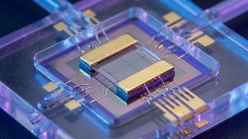
The most immediate practical application of this principle is the construction of an Encapsulated Graphene FET designed for high-frequency or low-noise applications. By sandwiching the graphene between two highly conductive layers, you create a controlled electrostatic environment where the carrier mobility is no longer dictated by distant substrate impurities, but by the local, screened environment you have engineered.
This architecture is particularly useful for:
1. High-frequency RF transistors where signal noise must be minimized.
2. Precision sensors where the baseline charge must be extremely stable.
3. Moiré-patterned devices (like twisted bilayer graphene) where the delicate electronic states are easily disrupted by external fields.
Required Materials and Equipment
Because this technique relies on precise geometry and high-quality interfaces, it is best suited for a small lab with cleanroom access.
1. Graphene: Chemical Vapor Deposition (CVD) grown graphene is preferred over exfoliated flakes for scalability, though exfoliated flakes offer higher initial mobility for prototyping.
2. Encapsulation Layer: Hexagonal Boron Nitride (hBN) is the industry standard. It is atomically smooth and provides an excellent dielectric environment.
3. Electrodes: Gold (Au) with a Titanium (Ti) adhesion layer is recommended for the conducting electrodes.
4. Substrate: Silicon with a thick thermal oxide layer (SiO2/Si) to act as a base.
5. Fabrication Tools: Electron-beam lithography (EBL) system, a metal evaporator (E-beam or Thermal), and a dry-transfer station for stacking 2D materials.
Prototype Fabrication Steps
The following steps outline the assembly of a screened graphene sandwich. Note that exact dimensions are not provided in the theoretical research; for a lab prototype, we assume an electrode separation of 100nm to 500nm to observe the transition from Coulomb to Yukawa-type interactions.
1. Substrate Preparation: Clean a Si/SiO2 substrate using standard RCA cleaning or oxygen plasma to remove organic contaminants.
2. Graphene Deposition: Deposit your CVD graphene onto the substrate. If using exfoliated graphene, use a mechanical transfer method to place it precisely.
3. First Electrode Layer: Use EBL to define the first set of electrodes. Evaporate a thin layer of Titanium followed by Gold. This layer will act as the bottom screening electrode.
4. Encapsulation Layer: Using a dry-transfer method, place a thin flake of hBN over the graphene. The thickness of this hBN layer will determine the distance at which the screening becomes dominant.
5. Second Electrode Layer: Repeat the EBL and evaporation process on top of the hBN layer. This creates the top electrode, completing the sandwich.
6. Contact Annealing: Perform a vacuum anneal (approximately 200 to 300 degrees Celsius) to improve the contact resistance between the metal electrodes and the graphene/hBN layers.
Testing and Characterization Plan
To verify that your device is operating under the predicted Yukawa-type interaction, you must perform a specific set of electrical tests.
1. DC Transport Measurements: Use a standard four-probe setup to measure the I-V (current-voltage) characteristics. Look for a reduction in the threshold voltage fluctuations compared to an unencapsulated device.
2. Carrier Mobility Calculation: Calculate the field-effect mobility. An increase in mobility compared to a standard substrate-supported device confirms that the screening is successfully mitigating charge-puddle interference.
3. Noise Spectroscopy: This is the most critical test. Measure the low-frequency noise power spectral density. A successful implementation of the screened architecture should show a significant reduction in the $1/f$ noise component, as the long-range interactions that drive charge fluctuations are suppressed.
4. Capacitance-Voltage (C-V) Profiling: Measure the capacitance of the device to determine the effective screening length. This will allow you to correlate the physical distance between your electrodes with the mathematical models of the Yukawa potential.
Engineering Risks and Mitigation
1. Interface Contamination: The biggest risk in 2D material fabrication is trapping air or hydrocarbons between the layers. This destroys the screening effect. Mitigation: Always use a dry-transfer method in an inert atmosphere (like a nitrogen glovebox) and perform rigorous plasma cleaning before metal deposition.
2. Contact Resistance: The electrodes must be in excellent electrical contact with the graphene. If the resistance is too high, the screening effect will be overshadowed by the device's internal resistance. Mitigation: Use a thin Titanium adhesion layer and perform a controlled thermal anneal.
3. Alignment Errors: In a sandwich geometry, the electrodes must be perfectly aligned to ensure the electric field is uniform across the graphene. Mitigation: Use high-resolution SEM (Scanning Electron Microscopy) to verify alignment before proceeding to metal deposition.
Source Basis and Assumptions
The engineering steps and material choices provided in this guide are based on industry-standard semiconductor fabrication techniques for 2D materials. The fundamental principle—that electrode encapsulation transforms Coulomb interactions into short-range Yukawa interactions—is derived from the theoretical models presented by Cancès, Gontier, and Perrin-Roussel.
Please note that while the research proves the mathematical stability (well-posedness) of these models, the specific dimensions (electrode spacing, hBN thickness) and the exact temperatures for annealing are engineering assumptions. For a first-time prototype, start with a larger electrode gap (500nm) to ensure device functionality before attempting to scale down to the sub-100nm regime where the Yukawa effects become most pronounced.
Evaluate Our Quality
Serious about B2B integration? Test our premium Pulsed Electrical Resistive Carbon Heating turbostratic graphene in your lab. 100g sample packs available now.