Quantum Currents in Bilayer Graphene: Unlocking Valleytronics via Magnetic Fields
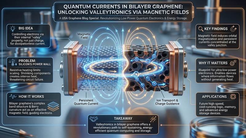
Imagine a computer chip that generates almost no heat because the electrons are not being pushed by a battery, but are instead flowing in a continuous, self-sustaining loop due to the very nature of the material they inhabit. This is not science fiction; it is the frontier of condensed matter physics. In the specialized world of two-dimensional materials, researchers are looking for ways to control electrons using their internal properties rather than just their electric charge. One of the most promising avenues involves using the valley degree of freedom in graphene. Recent theoretical work conducted by K. Shizuya explores how bilayer graphene, when engineered with a junction that separates two different valley states, reacts to a magnetic field. This research suggests that we can create persistent currents and localized magnetization at these junctions, providing a new way to store and move information at the quantum level.
The Problem This Research Is Solving
As the semiconductor industry approaches the physical limits of silicon-based technology, we face a massive engineering hurdle known as the power wall. In traditional transistors, information is processed by moving charge through a channel. This movement of charge inherently involves resistance, which leads to Joule heating. As we shrink these components to make them faster and more efficient, the heat generated per unit area becomes so intense that it threatens to melt the very circuits we are trying to build. This thermal bottleneck is a primary reason why we cannot simply continue scaling silicon indefinitely.
Beyond the heat problem, we are also running out of ways to encode information. Current electronics rely on the presence or absence of charge (binary 0 and 1). However, electrons possess other properties, such as spin and valley, which could theoretically allow for much denser and faster information processing. The challenge lies in how to create a junction or a boundary that can manipulate these properties without the massive energy loss associated with traditional charge-based currents. We need a way to control the flow of information that is topologically protected or driven by intrinsic quantum properties, rather than by brute-force voltage. This is where the study of bilayer graphene and its unique valley physics becomes essential for the future of computing.
The Key Idea in Plain English
To understand this research, we must first understand what a valley is in the context of a crystal. In a material like graphene, electrons do not behave like tiny billiard balls; they behave like waves. Because of the hexagonal arrangement of carbon atoms, these electron waves can have specific, stable patterns. There are two specific "valleys" in the energy landscape of graphene, which physicists call the K and K' valleys. You can think of these valleys as two different "flavors" or "states" that an electron can exist in.
The key idea being explored is "valleytronics." Just as spintronics uses the spin of an electron to represent data, valleytronics uses which valley the electron occupies. If we can create a junction—a boundary line—where the properties of the K valley on one side are different from the properties of the K valley on the other, we create a "valley-contrasting junction." When we apply a magnetic field to this junction, the magnetic field interacts with the electron's orbital motion. Because the two sides of the junction are fundamentally different in their quantum structure, the magnetic field induces a current that flows specifically along that boundary. This current is persistent, meaning it can flow without the continuous application of an external voltage, potentially revolutionizing how we think about energy consumption in nano-electronics.
How the Graphene-Based System Works
The mechanics of this system rely on the unique electronic band structure of bilayer graphene. Unlike monolayer graphene, which has a very simple energy landscape, bilayer graphene consists of two layers of carbon atoms stacked upon each other. This stacking, usually in an AB configuration, introduces a more complex relationship between the electrons and the crystal lattice. In this structure, the electrons have a property called Berry curvature.
Berry curvature is a geometric property of the electron's wave function in momentum space. You can think of it as a sort of "effective magnetic field" that the electron feels as it moves through the lattice, even when no external magnetic field is present. In bilayer graphene, the Berry curvature is highly dependent on the valley. In one valley, the curvature might be positive, while in the other, it is negative. This is the essence of the valley-contrasting junction.
When a magnetic field is applied to this junction, it introduces a Lorentz force that acts on the orbital motion of the electrons. Because the Berry curvature changes sign at the junction, the magnetic field interacts with the electrons differently on each side. This mismatch in the topological properties of the two sides creates a localized response. Specifically, the interaction between the external magnetic field and the intrinsic Berry curvature of the valleys generates an orbital magnetization. This magnetization is not caused by the electron's spin, but by the circular, loop-like motion of the electrons as they navigate the junction. This orbital motion results in a persistent current that flows along the interface of the junction. The cause is the interplay between the magnetic field and the topological mismatch of the valleys, and the effect is a localized, stable current.
What the Researchers Found
The research conducted by K. Shizuya provides a theoretical framework for understanding these complex interactions. The findings indicate that when a bilayer graphene system is configured with a valley-contrasting junction, the presence of an external magnetic field induces a specific type of orbital magnetization that is concentrated at the junction itself. This is a significant finding because it demonstrates that the junction acts as a localized source of magnetism and current.
Furthermore, the research explores the relationship between the strength of the magnetic field and the magnitude of the persistent current. The study suggests that the current is a direct consequence of the topological properties of the graphene layers. This means the current is intrinsically linked to the structure of the material itself. The results show that the magnetization is not just a bulk property of the material but is highly localized at the boundary where the valley properties change. This localization is critical for engineering, as it suggests that we could create very small, very precise "wires" of current that exist only at the edges of specifically engineered material boundaries.
Why the Result Matters
This research is significant because it provides a blueprint for a new type of electronic component. If we can successfully engineer these valley-contrasting junctions, we can create devices where information is carried by valley-states and persistent currents rather than by moving large amounts of charge. This could lead to a dramatic reduction in power consumption, as persistent currents do not require a continuous source of electrical potential to maintain their flow.
Moreover, the ability to generate localized magnetization through orbital motion rather than spin offers new ways to interact with magnetic memory and quantum bits. In the current landscape of technology, managing heat is the primary constraint on speed. By shifting the paradigm from charge-based movement to topological, valley-based currents, we bypass the primary driver of Joule heating. This opens the door to much higher integration densities, where components can be packed closer together without the risk of overheating, potentially allowing us to continue the trajectory of Moore's Law for many more years.
Limitations and What Still Needs Testing
While these theoretical findings are exciting, it is important to distinguish between a mathematical proof and a commercial product. Currently, this research remains in the realm of theoretical physics and computational modeling. Moving from a theoretical model to a physical device presents immense engineering challenges. First, the fabrication of a perfectly "valley-contrasting junction" is incredibly difficult. It requires atomic-scale precision to change the properties of the graphene layers at a specific boundary without introducing defects.
Defects are the enemy of quantum effects. Any impurity or structural flaw in the graphene lattice can cause "valley scattering," where an electron jumps from the K valley to the K' valley. This would effectively destroy the valley-contrasting nature of the junction and wipe out the persistent current. Additionally, these quantum effects are often observed at extremely low temperatures. In a real-world setting, thermal vibrations (phonons) can disrupt the delicate quantum states. For this research to have a practical business application, scientists will need to find ways to stabilize these currents at room temperature and develop scalable manufacturing techniques for creating these precise junctions in a mass-production environment.
Real-World Applications
The long-term applications for this technology are vast. In the field of quantum computing, the ability to create stable, localized currents and magnetization could lead to the development of new types of qubits. Qubits that are protected by the topological properties of the material (topological protection) are much less susceptible to the environmental noise that currently causes errors in quantum calculations.
In classical computing, "valleytronic" transistors could replace the standard field-effect transistors used in modern CPUs. These new transistors would operate based on the valley state of the electron, allowing for ultra-low-power logic gates. We also see potential in high-sensitivity magnetic sensors. Because the magnetization at these junctions is so sensitive to the local environment and the magnetic field, they could be used to create sensors for medical imaging or non-destructive testing in industrial settings. These sensors could potentially offer much higher resolution than current technology by operating at the quantum scale.
If You Remember One Thing
If you take away only one concept from this research, let it be this: the future of electronics may not depend on how much charge we can move, but on how we can manipulate the intrinsic quantum properties of materials like graphene to create efficient, self-sustaining currents.
FAQ
How is bilayer graphene different from normal graphene?
Bilayer graphene consists of two layers of carbon atoms stacked on top of each other. While monolayer graphene is a single atom thick, the addition of a second layer changes how the electrons behave, creating a more complex electronic structure that allows for new properties like the valley degree of freedom that we want to exploit for technology.
What exactly is a "valley" in an electronic context?
In a crystal lattice, electrons behave like waves. Because of the specific geometry of the carbon atoms, these waves have certain stable states that occur at specific points in their momentum. We call these points "valleys." Unlike a standard electrical charge, which is just a positive or negative value, a valley is a quantum state that can be used to encode information.
Why is a magnetic field necessary for this process?
The magnetic field acts as a catalyst that interacts with the unique geometry of the electron waves. Specifically, it interacts with the Berry curvature, which is a property of the graphene's electronic structure. This interaction causes the electrons to move in a specific way at the boundary where the valleys change, creating the persistent current and magnetization.
What is a persistent current and why is it useful?
A persistent current is a flow of electricity that continues to circulate in a loop without the need for an external power source, like a battery. This is a purely quantum mechanical effect. For electronics, this is incredibly useful because it means we could potentially move information with almost zero energy loss, drastically reducing the heat generated by computers.
Is this technology ready to be used in our smartphones?
Not yet. This research is currently in the theoretical and fundamental physics stage. To make it useful for consumer electronics, scientists first need to figure out how to manufacture these junctions perfectly and how to make these quantum effects work at room temperature without being disrupted by heat.
Conclusion
The research by K. Shizuya into bilayer graphene junctions represents a significant step forward in our understanding of how topology and magnetism can be combined at the nanoscale. By identifying how valley-contrasting junctions can host persistent currents and orbital magnetization, this work provides a theoretical foundation for the next generation of valleytronic devices. While significant engineering hurdles remain—particularly in fabrication and temperature stability—the potential to move beyond charge-based electronics and into a low-power, high-efficiency quantum era remains one of the most compelling goals in modern material science.
Evaluate Our Quality
Serious about B2B integration? Test our premium Pulsed Electrical Resistive Carbon Heating turbostratic graphene in your lab. 100g sample packs available now.