Decoding the Quantum Dance: How Electron Tomography Unlocks the Secrets of 2D Materials
Imagine you are standing on the edge of a perfectly still lake at twilight. You cannot see the water itself because it is too clear, but you can see how it reacts to the world. When a pebble drops into the water, it creates ripples that expand outward. If another pebble is dropped nearby, those ripples will collide, creating complex patterns of peaks and troughs where the waves overlap. By looking closely at these patterns of interference, a skilled observer could actually work backward to figure out how large the pebble was, how deep the water is, and even how fast the ripples are moving. This is the fundamental concept behind the cutting-edge research being conducted by A. Razanajatovo, J. Cayssol, and C. Dutreix. They are proposing a way to use these electronic ripples to create a complete, three-dimensional map of an electron's behavior. This process, known as electron state tomography, promises to turn the messy interference of quantum particles into a precise blueprint for the next generation of technology.
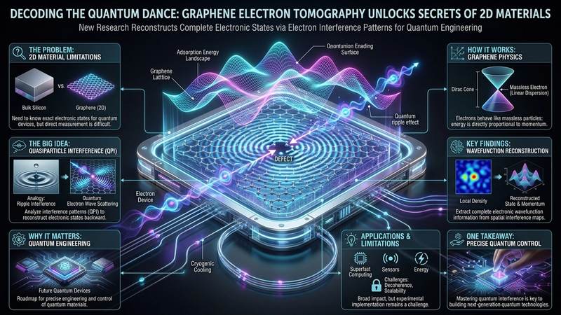
The Problem This Research Is Solving
In the pursuit of faster computers and more powerful quantum processors, scientists are moving away from traditional silicon-based semiconductors and toward two-dimensional materials like graphene. Graphene is a single layer of carbon atoms arranged in a hexagonal lattice, and its properties are extraordinary. However, to actually use these materials in real-world devices, engineers must understand exactly how electrons move through them. Specifically, they need to know the electronic states, which describe the energy and momentum of the electrons.
The current problem is that measuring these states directly is incredibly difficult. Traditional tools like the Scanning Tunneling Microscope (STM) allow scientists to see the surface of a material with incredible precision, but they typically only provide a measurement of the local density of states. This essentially tells you where the electrons are likely to be at a specific point, but it does not provide a complete picture of their momentum or their full wave-like nature. This is a massive limitation because the behavior of a quantum device depends not just on where the electrons are, but on how they move and how they interact with one another. Without a complete map of these states, designing advanced electronics becomes a process of trial and error rather than precise engineering. We are essentially trying to design a complex engine while only being able to see snapshots of where the parts are, rather than seeing the full, continuous motion of the machinery.
The Key Idea in Plain English
The researchers suggest a way to bypass this limitation by looking at the interference patterns created by quasiparticle interference, or QPI. When an electron travels through a material, it behaves like a wave. If that electron encounters a defect—such as a missing atom, a different type of atom, or a physical edge in the material—the electron wave scatters. This scattering causes the electron wave to bounce off the defect and overlap with the original wave.
This overlap creates a standing wave pattern of high and low electron density, much like the ripples in the lake mentioned earlier. These patterns are not random noise; they are highly structured and contain encoded information about the electronic states of the material. The key idea is that if we can capture a sufficiently detailed map of these interference patterns across a surface, we can use a mathematical process called tomography to reconstruct the full electronic wavefunction. In medical imaging, tomography uses X-rays from many angles to create a 3D image of a body. In this scientific context, electron state tomography uses the spatial patterns of electron interference to reconstruct the momentum-dependent electronic states of the material.
How the Graphene-Based System Works
To understand how this works, we have to look at the unique physics of graphene. In most materials, electrons behave like tiny balls with mass. However, in graphene, the electrons behave as if they have no mass at all. This phenomenon, caused by the unique hexagonal structure of the carbon lattice, means that their energy is directly proportional to their momentum. This relationship is known as a linear dispersion relation, and it is often visualized as a cone-shaped energy landscape called a Dirac cone.
Because these electrons behave as massless particles, their scattering patterns are very distinct. When an electron wave hits a defect, the scattering amplitude is dictated by the specific electronic structure of the material. This scattering is described mathematically by the interaction between the electron's wave function and the potential created by the defect. The resulting interference pattern is a spatial representation of the material's momentum-space properties.
The measurement process involves using a Scanning Tunneling Microscope to scan a tip over the surface of the graphene. As the tip moves, it measures the local density of states at every point, effectively capturing the interference pattern. Once this spatial map is collected, the researchers apply a mathematical transformation, often involving a Fourier transform, to move the data from real space (the physical surface) into momentum space (the energy and movement of the electron). By analyzing how the intensity of the interference changes across different locations, the tomography algorithm can reconstruct the full electronic state, providing both the position and the momentum information that was previously missing.
What the Researchers Found
The work of Razanajatovo, Cayssol, and Dutreix provides a theoretical framework that demonstrates how these interference maps can be used to extract the complete electronic wavefunction. Their findings suggest that the information required for a full reconstruction is indeed embedded within the spatial variations of the quasiparticle interference patterns.
Crucially, the research shows that we are not limited to just seeing where the electrons are (the local density of states). Instead, by analyzing the specific way these waves interfere, we can reconstruct the underlying momentum-resolved electronic structure. This means the researchers have identified a mathematical bridge that connects the visible interference patterns seen in a microscope to the invisible, fundamental movements of the electrons. This move from simple density mapping to full state tomography represents a significant leap in how we can interpret data from scanning probes.
Why the Result Matters
This research is significant because it provides a roadmap for the precise engineering of quantum materials. As we transition from classical electronics to quantum-scale devices, the ability to control individual electron states becomes paramount. For example, in the field of valleytronics, researchers aim to use the "valley" degree of freedom in graphene—a property related to the electron's momentum—to store and process information. This is similar to how traditional electronics use the charge of an electron. To make valleytronics a reality, we must be able to see and manipulate these valleys with absolute precision.
Furthermore, this technique allows for a much deeper understanding of how defects affect material performance. In traditional manufacturing, a defect is simply a failure. In quantum engineering, a defect can be a tool; by strategically placing specific atoms or creating specific edges, engineers can create "channels" or "traps" for electrons. This research provides the diagnostic tool needed to verify that these engineered defects are behaving exactly as intended, allowing for the design of sophisticated, programmable quantum landscapes.
Limitations and What Still Needs Testing
While the theoretical framework is robust, there are significant practical hurdles that remain. First, the accuracy of the reconstruction is heavily dependent on the quality of the initial image. Any noise in the measurement, whether from thermal vibrations or electronic interference, can lead to errors in the reconstructed state. Achieving the level of resolution required for true tomography requires extremely stable, ultra-low-temperature environments to minimize thermal noise.
Second, the computational complexity of reconstructing a full wavefunction from complex interference patterns is immense. As the size of the area being scanned increases, the amount of data and the mathematical processing power required grow exponentially. Finally, while the theory works beautifully for idealized models of graphene, real-world materials are often much messier. They contain unintended impurities, substrate interactions, and structural twists that can complicate the interference patterns and make the mathematical reconstruction much more difficult to achieve in a laboratory setting.
Real-World Applications
The ability to map electron states through tomography has profound implications for several high-tech industries. In the semiconductor industry, it could lead to a new era of design where atomic-scale defects are used to create ultra-efficient transistors that operate at much lower power than current silicon models.
In the burgeoning field of quantum computing, this technique could be used to characterize the states of qubits in solid-state systems. To build a scalable quantum computer, we need to know exactly how the quantum information (the state) is being maintained and how it is being disturbed by its environment. Electron state tomography could provide the high-resolution diagnostic needed to ensure quantum coherence.
Additionally, advanced sensing technologies could benefit from this research. Sensors that rely on the quantum properties of electrons, such as highly sensitive magnetic or electrical field detectors, require a deep understanding of the material's electronic state to maximize their sensitivity and reduce noise.
If You Remember One Thing
If you remember only one thing from this research, let it be this: We are moving toward a future where we no longer have to guess how electrons behave in new materials; instead, we can use the interference patterns they leave behind to reconstruct their complete, detailed blueprints, allowing us to engineer the quantum world with unprecedented precision.
FAQ
What is the difference between local density of states and full electron state tomography?
Local density of states tells us the probability of finding an electron at a specific location and energy, but it lacks information about the electron's momentum. Electron state tomography goes further by using interference patterns to reconstruct the full wavefunction, which includes both the location and the momentum of the electron, providing a complete picture of its state.
Why is graphene such a popular subject for this kind of research?
Graphene is ideal because its electrons behave as massless particles with a linear energy-momentum relationship. This unique property makes the interference patterns created by scattering much more distinct and mathematically predictable than in traditional materials, making it easier to apply tomographic reconstruction techniques.
Can this technique be used on materials other than graphene?
Yes, the theoretical framework is not limited to graphene. While graphene's unique properties make it an excellent starting point, the principles of quasiparticle interference and tomography can, in theory, be applied to any two-dimensional material or even three-dimensional crystals, provided the interference patterns can be captured with sufficient resolution.
What kind of microscope is needed to perform these measurements?
A Scanning Tunneling Microscope (STM) is the primary tool used for this. An STM uses a very sharp metallic tip that is brought incredibly close to a surface, allowing electrons to "tunnel" between the tip and the sample. This allows for the atomic-scale resolution necessary to see the tiny interference patterns caused by electron scattering.
Is this technology ready for use in making consumer electronics?
Not yet. Currently, this research is at a fundamental, theoretical, and laboratory stage. The requirements for extremely low temperatures, high vacuum, and specialized scanning equipment mean that this is a research tool for scientists rather than a manufacturing tool for factories. However, it is a critical step toward enabling the next generation of electronic technologies.
Conclusion
The work of Razanajatovo, Cayssol, and Dutreix represents a significant shift in how we approach the study of condensed matter physics. By turning the "noise" of electron scattering into a source of detailed information, they have provided a way to peer into the very heart of electronic behavior. As we continue to master the art of the two-dimensional world, the ability to reconstruct the complete electronic state through tomography will be a cornerstone of both fundamental discovery and the engineering of the quantum future.
Evaluate Our Quality
Serious about B2B integration? Test our premium Pulsed Electrical Resistive Carbon Heating turbostratic graphene in your lab. 100g sample packs available now.