Practical Guide: Engineering Valley-Polarized Electron Optics using Bilayer Graphene Quantum Dots
The Shift from Spintronics to Valleytronics
In traditional semiconductor engineering, information is processed using the charge or the spin of an electron. However, graphene offers a third degree of freedom: the valley index. In bilayer graphene (BLG), electrons occupy two distinct energy minima in momentum space, known as valleys.
The research by Ildarabadi and Power (2026) provides a blueprint for controlling these valleys using nothing more than electrostatic gating. By applying an asymmetric voltage between the top and bottom gates of a Bernal-stacked bilayer graphene flake, you can create a local mass-like term that has opposite signs for each valley. This effectively turns a quantum dot into an optical element for electrons, allowing you to steer, split, or filter electron beams based on their valley index without the need for bulky magnetic fields or complex strain engineering.
This guide outlines how to prototype a valley-dependent electron optical element, specifically focusing on a valley-polarized splitter.
Required Materials and Device Architecture
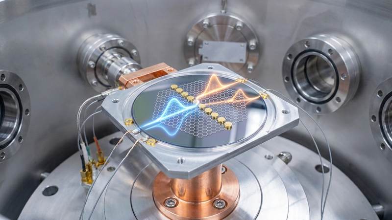
To implement this, you cannot use standard monolayer graphene. You must use Bernal-stacked bilayer graphene (BLG) to take advantage of the tunable bandgap and the valley-dependent mass term.
The device must be a van der Waals heterostructure consisting of the following layers:
- Substrate: Silicon/Silicon Dioxide (Si/SiO2) or a specialized sapphire substrate.
- Encapsulation/Dielectric: Hexagonal Boron Nitride (hBN). High-quality, atomically flat hBN is mandatory to maintain high electron mobility.
- Active Layer: Bernal-stacked Bilayer Graphene (BLG).
- Top Gate: A thin layer of hBN or a metallic gate electrode separated by a dielectric.
- Bottom Gate: A global or local back-gate, typically a highly doped Si substrate or a dedicated metal gate.
- Contacts: Palladium (Pd) or Gold (Au) for low-resistance electrical connections.
The architecture must be dual-gated. The ability to apply different voltages to the top and bottom gates (layer-antisymmetric gating) is the fundamental requirement for generating the valley-dependent scattering mechanism.
Fabrication Workflow
Building a device capable of observing valley-dependent optics requires precision assembly, typically via a dry-transfer method in an inert atmosphere (Glovebox) to prevent contamination.
1. Substrate Preparation: Clean the Si/SiO2 substrate using oxygen plasma to ensure optimal adhesion of the first hBN layer.
2. Layer Stacking: Using a polymer-based transfer method (such as PC or PDMS), stack the layers in the following order: Substrate / hBN (bottom dielectric) / Bilayer Graphene / hBN (top dielectric) / Top Gate Electrode.
3. Device Patterning: Use Electron Beam Lithography (EBL) to define the geometry of the quantum dots. The dots must be small enough to act as localized scattering centers (typically sub-micron in diameter) but large enough to be defined by the gate geometry.
4. Gate Electrode Deposition: Deposit the top gate material using electron beam evaporation. If using a metal top gate, ensure the dielectric layer (hBN) is thick enough to prevent tunneling/leakage but thin enough to allow effective electrostatic control.
5. Contact Metallization: Pattern the source and drain contacts using EBL and metal evaporation. Palladium is preferred for graphene to ensure a low-contact resistance, which is critical for observing quantum transport effects.
6. Final Encapsulation: If the device is not already fully encapsulated, perform a final hBN encapsulation to protect the graphene from atmospheric degradation.
Engineering the Optical Elements
Once the device is fabricated, you can program its function by adjusting the gate voltages. The research identifies three specific configurations:
- Valley Deflector: Apply a single, localized asymmetric voltage to a single quantum dot. This will cause an incoming electron beam to deflect at different angles depending on its valley index.
- Valley Splitter: Arrange two identical quantum dots in a series. When an electron beam passes through this array, the valley-dependent scattering will cause the two valleys to diverge, effectively splitting the current into two distinct paths.
- Valley Filter: Arrange two quantum dots with opposite gating profiles (one with $V_{top} > V_{bottom}$ and the other with $V_{top} < V_{bottom}$). This configuration will suppress the transmission of one valley while allowing the other to pass, resulting in a highly valley-polarized current.
Testing and Validation Protocol
Validating valley-polarized transport is challenging because standard electrical probes do not distinguish between valleys. To test this prototype, you should use a multi-terminal geometry.
1. Baseline Characterization: Before applying asymmetric gating, measure the longitudinal resistance ($R_{xx}$) and Hall resistance ($R_{xy}$) to ensure the BLG mobility is sufficiently high (ideally $> 10,000 cm^2/Vs$ at low temperatures).
2. Asymmetric Gate Sweep: Gradually increase the difference between the top and bottom gate voltages ($\Delta V = V_{top} - V_{bottom}$). Monitor the conductance of the device.
3. Transverse Current Measurement: Use a multi-terminal setup (e.g., a Hall bar geometry with additional side probes) to detect transverse voltage or current. As the valley-dependent scattering increases, you should observe a deviation in the expected current distribution, indicating that the electron paths are being deflected.
4. Temperature Dependence: Perform measurements in a cryostat. While the paper suggests the effect is accessible, the quantum dot effects and valley coherence are most pronounced at low temperatures (typically below 4K).
Engineering Assumptions and Known Variables
Since this is a cutting-edge implementation, the following parameters are assumed based on the research and standard BLG physics:
- Gate Voltages: The asymmetry required to open a significant gap is assumed to be in the range of 1V to 10V, depending on the thickness of the hBN dielectric.
- Dot Dimensions: The quantum dots are assumed to be between 100nm and 500nm in diameter.
- Operating Temperature: While the theory is robust, experimental verification is assumed to require liquid Helium temperatures (approx. 4K) to minimize thermal broadening of the energy levels.
- Dielectric Thickness: The hBN layers are assumed to be between 10nm and 30nm. Thinner layers allow for stronger gating but increase the risk of gate leakage.
Technical Risks and Mitigation
- Fabrication Complexity: The primary risk is the misalignment of the dual gates during the transfer process. Mitigation: Use high-resolution EBL and perform SEM (Scanning Electron Microscopy) inspections at every stacking step.
- Gate Leakage: Applying high asymmetric voltages can cause dielectric breakdown. Mitigation: Use high-quality, single-crystal hBN and perform leakage current tests at low voltages before full-scale operation.
- Thermal Decoherence: If the temperature is too high, the electron's phase coherence is lost, and the "optical" behavior disappears. Mitigation: Ensure the device is properly thermalized to the mixing chamber of a dilution refrigerator or a liquid Helium cryostat.
- Contact Resistance: High resistance at the source/drain can mask the subtle valley-dependent signals. Mitigation: Use Palladium contacts and optimize the annealing process during metallization.
Evaluate Our Quality
Serious about B2B integration? Test our premium Pulsed Electrical Resistive Carbon Heating turbostratic graphene in your lab. 100g sample packs available now.