Beyond Silicon: Using Graphene to Unlock the Full Potential of Nitride Solar Cells
The future of renewable energy depends on our ability to squeeze every possible drop of energy from the sun. While silicon-based solar cells dominate our rooftops today, they are reaching their physical limits. Scientists are now looking toward next-generation materials like nitrides, which offer much higher stability and performance in extreme conditions. However, a major hurdle remains: how do you collect electricity from these materials without blocking the very sunlight they need to function? This is where the unique properties of graphene come into play. By using a single, atomic-thin layer of carbon, researchers have found a way to create a window that is both perfectly clear and incredibly conductive. This breakthrough, explored in recent studies, suggests a new path for solar technology that could be more efficient and more durable than anything we currently use.
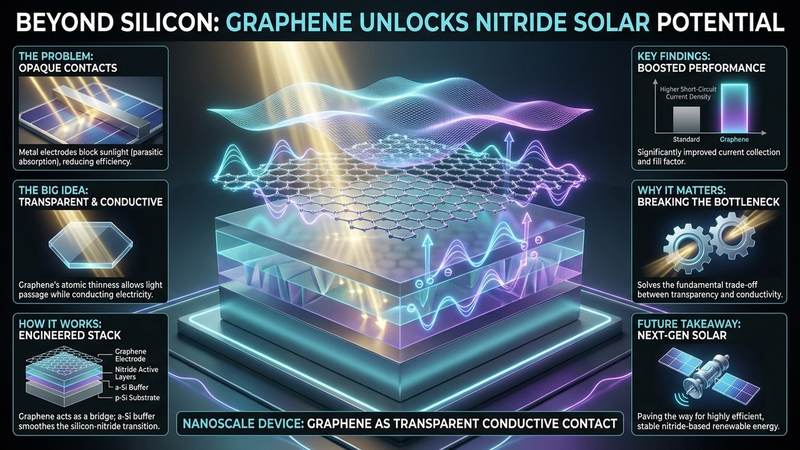
The Problem This Research Is Solving
Traditional solar cells rely on metal contacts to pull electricity out of the semiconductor material. While metals are excellent conductors, they are also opaque. When you place a thick layer of metal on top of a solar cell, it acts like a shade, blocking a significant portion of incoming sunlight from ever reaching the active layers of the device. This phenomenon, known as parasitic absorption, directly reduces the amount of energy the cell can generate. To solve this, engineers often turn to transparent conductive oxides. While these materials are indeed clear, they often suffer from high electrical resistance or are quite expensive to manufacture at scale. This creates a fundamental conflict in solar cell design: you can have a material that is highly conductive but blocks light, or a material that is highly transparent but resists the flow of electricity.
Furthermore, the development of nitride-based solar cells, such as those using aluminum indium nitride (AlInN), presents its own set of structural challenges. These materials are often grown on silicon substrates to keep costs low. However, the atomic arrangement of silicon does not match the atomic arrangement of nitrides very well. This mismatch creates a high density of defects at the interface where the two materials meet. These defects act as traps for electrons, causing them to recombine and disappear before they can be harvested as electricity, which drastically lowers the efficiency of the cell.
The Key Idea in Plain English
The solution proposed by the scientific community involves a revolutionary material called graphene. Graphene is a single layer of carbon atoms arranged in a hexagonal lattice. It is one of the thinnest materials in existence, yet it is incredibly strong and possesses extraordinary electrical conductivity. Because it is only one atom thick, it is almost entirely transparent, allowing sunlight to pass through it with minimal loss.
The core idea is to use graphene as a semitransparent electrode. Instead of using an opaque metal or a resistive oxide, the graphene acts as a highly efficient bridge. It allows light to reach the semiconductor layers while simultaneously providing a high-speed highway for the electrons to escape the cell and enter the external circuit. By integrating this atomic-scale layer, scientists aim to bypass the traditional trade-off between light absorption and electrical collection, effectively solving the parasitic absorption problem while simultaneously lowering the resistance of the device.
How the Graphene-Based System Works
The system described in this research utilizes a sophisticated semiconductor architecture to maximize performance. The foundation of the device is a p-type silicon substrate, which serves as the base. To solve the issue of structural defects caused by the mismatch between silicon and the nitride layers, researchers incorporate a thin buffer layer of amorphous silicon, known as a-Si. This buffer layer acts as a structural mediator, smoothing out the atomic transition between the silicon base and the complex nitride layers above it. This step is vital because it minimizes the number of electron traps at the interface, ensuring that the charge carriers can move more freely.
On top of this buffer, layers of AlInN are deposited. The composition of these layers is critical, as the ratio of aluminum to indium determines the bandgap of the material. The researchers investigated three specific compositions: x=0.22, x=0.35, and x=0.43. By varying the aluminum content, they could tune the electrical properties of the cell to see which configuration worked best with the graphene layer.
The final, most important component is the graphene itself. Using a low-temperature transfer process, a monolayer of graphene is placed onto the front surface of the AlInN layers. This process is specifically chosen because high temperatures can damage the sensitive semiconductor layers or the delicate buffer interface. Once the graphene is in place, it forms a semitransparent conductive contact. When sunlight hits the cell, the photons pass through the graphene and are absorbed by the AlInN layers, creating electron-hole pairs. The graphene then collects these electrons with very little resistance, pulling them out of the cell to create a usable electric current.
What the Researchers Found
The research, conducted by Miriam Cadenas, Mireia Martínez, Kerly Sánchez, Jordi Ibáñez, Sergi Hernández, Sirona Valdueza-Felip, Ana M. Diez-Pascual, and Fernando B. Naranjo, yielded significant results across all tested material compositions. The most striking finding was the improvement in the short-circuit current density, which is the maximum current the cell can produce when the voltage is zero. This improvement occurs because the graphene layer is much more transparent than traditional metal contacts, allowing more photons to reach the active semiconductor material.
In addition to current, the fill factor of the solar cells showed a clear and consistent improvement. The fill factor is a measure of the quality of the solar cell, essentially describing how close the device's performance is to an ideal rectangular curve. A higher fill factor indicates lower internal resistance. The graphene layer successfully reduced the series resistance of the device, making it much easier for the generated electricity to flow out of the cell without being lost to heat.
The overall power conversion efficiency, which is the total amount of sunlight converted into usable electricity, also saw a marked increase across all aluminum compositions (x=0.22, 0.35, and 0.43). It is important to note, however, that the open-circuit voltage remained largely unaffected. The open-circuit voltage is determined by the fundamental physics of the semiconductor junction and the material's bandgap. Since the graphene layer is a surface contact and does not change the internal chemistry or the bandgap of the AlInN itself, the voltage produced by the junction stays the same, even as the current and efficiency rise.
Why the Result Matters
This research is significant because it addresses the fundamental "transparency-conductivity" bottleneck in solar cell engineering. By proving that graphene can act as an effective contact for nitride-based cells, the study provides a blueprint for increasing the efficiency of a wide range of semiconductor technologies. Nitride-based solar cells are particularly interesting because they are much more robust than standard silicon cells. They can operate at much higher temperatures and are more resistant to environmental degradation, making them ideal for concentrated solar power or space-based applications.
The ability to use a low-temperature transfer process to apply graphene is also a major practical win. In semiconductor manufacturing, heat is often a destructive force that can ruin the delicate layers of a device. A process that works at low temperatures makes the integration of graphene much more viable for industrial production. If we can successfully scale this technology, we could see a new generation of high-efficiency solar panels that are not only more powerful but also more durable in harsh environments.
Limitations and What Still Needs Testing
While the results are highly promising, it is important to maintain a realistic perspective on the current state of this technology. This research is a fundamental scientific study, not a report on a commercially ready product. One of the primary challenges remains the scalability of the graphene transfer process. While transferring a single layer of graphene in a laboratory setting is possible, doing so uniformly and without defects over large, meter-wide solar panels is an immense engineering challenge. Any tiny tear or wrinkle in the graphene layer could create a point of high resistance or a spot where light is blocked.
Furthermore, the long-term stability of the graphene-semiconductor interface under constant exposure to UV light and moisture has not been fully explored in this specific study. Graphene is a stable material, but the interface between the carbon layer and the nitride layer must be able to withstand decades of environmental stress to be viable for consumer use. Future research will need to focus on "encapsulation" techniques that protect the graphene and the underlying semiconductor while still allowing light to pass through.
Real-World Applications
The successful implementation of graphene-based nitride solar cells could lead to breakthroughs in several specialized sectors. In the field of concentrated photovoltaics (CPV), where sunlight is focused through lenses onto a small cell, the ability to handle high heat and maintain high efficiency is critical. Nitride cells are naturally suited for this, and graphene would enhance their ability to extract current in these high-intensity environments.
Another exciting application is in the realm of tandem solar cells. These are devices that stack multiple different semiconductor materials on top of each other to capture different parts of the light spectrum. Graphene's unique ability to be both transparent and conductive makes it the perfect candidate for the "interconnect" layers in these multi-junction stacks, potentially pushing solar efficiency toward the theoretical limits. Additionally, because nitrides are quite rugged, these cells could find specialized use in aerospace or satellite technology, where reliability and high-performance per unit of area are more important than the initial cost of materials.
If You Remember One Thing
If you take away only one concept from this research, let it be this: graphene solves the solar cell dilemma by acting as a transparent highway, allowing light to enter while simultaneously providing a high-speed path for electricity to exit, thereby increasing overall efficiency without sacrificing transparency.
FAQ
What exactly is graphene and why is it special for solar cells?
Graphene is a single layer of carbon atoms arranged in a hexagonal pattern. It is special because it is incredibly thin, allowing it to be almost perfectly transparent, yet it is one of the best conductors of electricity known to science. In solar cells, this means it can collect electricity without blocking the sunlight.
Why are nitride-based solar cells better than the silicon ones we use now?
Nitride-based solar cells, like the AlInN studied here, are much more stable and can operate at much higher temperatures than standard silicon cells. This makes them much more useful for industrial applications or environments where the sun is very intense and the heat is high.
Why did the researchers use a buffer layer instead of just putting the nitride on silicon?
When you put two different materials together, like silicon and nitrides, their atoms don't always line up perfectly. This mismatch causes defects that trap electricity. The amorphous silicon buffer layer acts as a smooth transition zone, reducing these defects and helping the electricity flow more smoothly.
The research says the voltage didn't change much. Does that mean the graphene didn't help?
The graphene definitely helped, but it helped in different ways. The voltage is mostly determined by the internal chemistry of the semiconductor itself. The graphene improved the current and the overall efficiency by making it easier for the charge to flow and by letting more light in, which is different from changing the voltage.
Is this technology going to be on my roof next year?
Not quite yet. While the science is very promising, moving from a successful laboratory experiment to a mass-produced commercial product is a huge step. Engineers still need to figure out how to manufacture large sheets of graphene perfectly and how to protect it from the weather for twenty years.
Conclusion
This research points toward a practical lesson: graphene-based materials are most powerful when their nanoscale properties are connected to a clear engineering problem. The result is not a finished commercial product by itself, but it gives researchers and manufacturers a better map for designing lighter, more sensitive, or more durable systems. Future work still needs testing under real operating conditions, but the direction is promising because it joins materials science with application-driven design.
Evaluate Our Quality
Serious about B2B integration? Test our premium Pulsed Electrical Resistive Carbon Heating turbostratic graphene in your lab. 100g sample packs available now.