Mapping the Hidden Third Dimension of Twisted 2D Crystals
Imagine taking two identical sheets of fine chicken wire and laying one directly on top of the other. If they are perfectly aligned, you see a simple, predictable grid. But if you rotate one sheet by just a few degrees, a startling new pattern emerges across the surface. This is known as a moiré pattern, and in the world of nanotechnology, it is much more than a visual curiosity. These patterns create entirely new environments for electrons, potentially enabling a new era of quantum computers and ultra-efficient electronics. However, there has been a massive mystery at the heart of this phenomenon. While we can see these patterns, we have struggled to see exactly how the atoms themselves shift in three dimensions to create them.
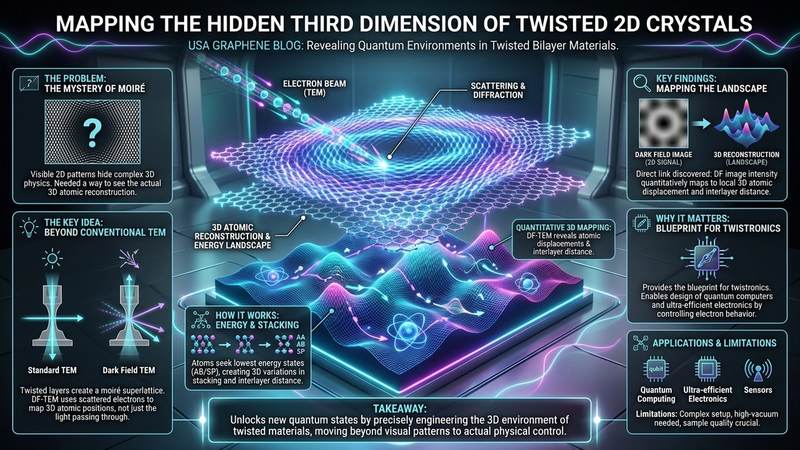
The Problem This Research Is Solving
For years, scientists have been captivated by the emergence of exotic physical states in twisted bilayer materials. When two layers of a material, such as graphene or transition metal dichalcogenides, are twisted relative to each other, they create a moiré superlattice. This new structure possesses a much larger periodicity than the original atomic lattice, which fundamentally changes how electrons behave. For example, in twisted bilayer graphene, this phenomenon can lead to the formation of flat bands, where electrons move very slowly and begin to interact with each other in intense, complex ways. In other materials, it can lead to Wigner crystallization, where electrons arrange themselves into a rigid grid like a crystal of salt.
Despite the excitement surrounding these phenomena, a significant hurdle remains. Most of our observation techniques are limited to a two-dimensional view. We can see the in-plane displacements—the way atoms shift left, right, up, or down within the plane of the sheet. However, we have lacked a reliable way to observe the three-dimensional reality of these structures. In a twisted bilayer, the atoms do not simply remain in two perfectly flat, parallel planes. To minimize the total energy of the system, the atoms undergo a process called reconstruction. They buckle, shifting slightly up or down to find the most stable stacking configuration. Without knowing the exact vertical positions and the precise interlayer distances, we are essentially trying to solve a complex mathematical equation while missing half of the variables. This lack of 3D data prevents researchers from building accurate models to predict the electronic properties of these materials, effectively slowing the development of twistronics.
The Key Idea in Plain English
The breakthrough comes from a sophisticated evolution of a technique known as dark field transmission electron microscopy. To understand this, we first need to understand how a standard electron microscope works. A standard microscope shoots a beam of electrons through a very thin sample. As the electrons pass through the atoms, they are scattered in different directions based on the atomic arrangement. By looking at how these electrons are deflected, we can map out where the atoms are.
In conventional transmission electron microscopy, we usually look at the light that passes straight through the sample. However, in dark field microscopy, we do not look at the direct beam. Instead, we use a specialized lens to select only the electrons that have been scattered at a very specific angle. This specific angle corresponds to a particular orientation of the atomic lattice. Because only electrons scattered by a specific atomic alignment reach our detector, the image becomes highly sensitive to any deviations in that alignment. The researchers realized that the intensity of the light in a dark field image is not just a random brightness; it is directly tied to the local stacking order of the atoms. By analyzing how this intensity fluctuates across the moiré pattern, we can mathematically reconstruct the three-dimensional architecture of the entire system.
How the Graphene-Based System Works
To understand why reconstruction occurs, we must look at the energy landscape of a twisted bilayer. When two layers are twisted, they create a landscape of different stacking regions. Some areas might have AA stacking, where atoms in the top layer sit directly above atoms in the bottom layer. Other areas might have AB or SP stacking, where atoms sit in the "valleys" between the atoms of the layer below.
The energy of these different stacking configurations is not equal. In many materials, certain stacking orders are much more stable than others. Because nature always seeks the lowest energy state, the atoms will physically move to expand the regions of stable stacking and minimize the regions of unstable stacking. This movement is the reconstruction. As the atoms shift to reach these stable zones, they do not just move sideways; they also move vertically. They might bulge upward or dip downward to accommodate the shift in the lateral grid. This creates a corrugated, undulating surface at the atomic scale. This vertical movement, or the change in interlayer distance, is a critical component of the moiré superlattice because it alters the electronic coupling between the two layers. The stronger the overlap between the electron clouds of the two layers, the more significant the effect on the material's conductivity and quantum properties.
What the Researchers Found
The research team, including Pankaj Kumar, Michel Bosman, Nikolai Lavrentev, He Zheng, Ding Peng, Kostya S. Novoselov, and Tatiana Latychevskaia, successfully demonstrated that dark field microscopy can be used to extract both the 3D atomic displacements and the interlayer distance. They proved that there is a direct, quantitative relationship between the intensity of the signal in a dark field image and the local stacking configuration of the atoms.
By measuring these intensities across the entire moiré pattern, the researchers were able to map out the three-dimensional "landscape" of the twisted bilayer. They showed that they could determine exactly how much the atoms buckle and how the distance between the two sheets fluctuates from one point to another. This is a monumental shift from previous methods that could only provide a simplified, two-dimensional approximation. Essentially, they turned a 2D imaging tool into a 3D topographical map of the atomic scale. This allows us to see the "valleys" and "peaks" created by the atomic reconstruction with unprecedented precision.
Why the Result Matters
This discovery is a cornerstone for the future of material science because it provides the missing blueprint for twistronics. In the past, scientists had to rely on complex computer simulations to guess what the 3D structure of a twisted crystal looked like. These simulations were often difficult to verify because there was no direct experimental way to check the results. Now, we have a way to verify those models with real-world measurements.
When we know the exact 3D positions of every atom, we can precisely calculate the electronic band structure of the material. This is essential because the electronic properties—such as whether a material is a metal, a semiconductor, or a superconductor—are extremely sensitive to the exact distance between the layers and the local atomic arrangement. For instance, if we want to engineer a material to have specific quantum properties, such as a specific type of topological insulator behavior, we need to know exactly how to twist the layers and how they will reconstruct. This research provides the toolset needed to move from observing phenomena to engineering them with mathematical certainty.
Limitations and What Still Needs Testing
While this work is a significant leap forward, it is not a magic wand that solves all problems in 2D materials. One of the primary challenges in electron microscopy is the destructive nature of the electron beam itself. High-energy electrons are used to image the atoms, but these same electrons can knock atoms out of place or damage the delicate van der Waals bonds between layers. This phenomenon, known as radiation damage, can alter the very structure the researchers are trying to measure. Future work must focus on how to perform these 3D reconstructions using even lower electron doses or more advanced direct electron detectors to minimize damage.
Furthermore, while the technique works beautifully on specific materials like graphene and certain transition metal dichalcogenides, the complexity of the mathematics required to reconstruct 3D structures increases significantly with more complex crystal systems. Applying this method to more exotic or multi-layer heterostructures will require even more sophisticated computational models. Finally, the process of preparing the samples—making them thin enough for electrons to pass through while keeping them perfectly intact—remains a highly delicate and difficult task that limits how widely this technique can be applied in a standard lab setting.
Real-World Applications
The implications for real-world technology are profound. In the realm of quantum computing, the ability to control and predict the behavior of electrons in moiré superlattices could lead to the creation of more stable qubits. These qubits would be less susceptible to environmental noise because their properties are protected by the unique topology of the twisted lattice.
In the semiconductor industry, this research could pave the way for a new class of "twistronic" transistors. Current silicon-based transistors are reaching their physical limits. By using twisted 2D materials, we might be able to create electronic components that are not only smaller but also have entirely different switching mechanisms, such as those based on topological phases. This could lead to processors that are much faster and consume significantly less power. Additionally, the high sensitivity of these moiré patterns to external influences like pressure or electric fields makes them ideal candidates for next-generation sensors, capable of detecting single molecules or extremely subtle changes in their environment.
If You Remember One Thing
If you take away only one concept, let it be this: the properties of twisted 2D materials are driven by a hidden three-dimensional architecture, and we finally have a way to see it.
FAQ
What is a moiré pattern? A moiré pattern is a visual effect that occurs when two similar patterns, such as the atomic grids of two sheets of graphene, are overlaid at a slight angle. This creates a new, much larger pattern that can significantly change the physical and electronic properties of the material.
How does dark field TEM work? Dark field transmission electron microscopy works by using a specialized lens to select only electrons that have been scattered at a very specific angle. Instead of looking at the main beam of electrons, you look at these specifically scattered electrons, which makes the image highly sensitive to the exact arrangement and orientation of the atoms.
Why do atoms move when layers are twisted? Atoms naturally seek the state of lowest energy. When layers are twisted, the atoms in the top and bottom layers don't always fit together perfectly. To find the most stable, low-energy configuration, the atoms shift sideways and move up or down to maximize favorable connections between the layers.
Is this technique used for all 2D materials? While the principles are universal, the technique is currently most effective for specific materials like graphene and transition metal dichalcogenides. Applying it to more complex materials is challenging due to the potential for electron beam damage and the increasing mathematical complexity of the reconstruction.
How does this help in making better electronics? By allowing us to see the exact 3D structure of twisted materials, we can accurately predict how they will conduct electricity. This allows scientists to design and engineer new materials with specific, pre-planned electronic properties, which is essential for creating faster, smaller, and more efficient quantum and semiconductor devices.
Conclusion
The ability to untangle the three-dimensional atomic reconstruction of twisted bilayer crystals marks a turning point in condensed matter physics. By bridging the gap between two-dimensional observations and the true three-dimensional reality of atomic structures, researchers have provided the tools necessary to transform twistronics from a field of observation into a field of precise engineering. As we refine these techniques and overcome the challenges of electron beam damage, the ability to manipulate these complex, undulating atomic landscapes will undoubtedly lead to a new generation of quantum technologies and electronic devices.
Evaluate Our Quality
Serious about B2B integration? Test our premium Pulsed Electrical Resistive Carbon Heating turbostratic graphene in your lab. 100g sample packs available now.