Practical Guide: Engineering Strain-Tunable IR Sensors Using Edge-Modified Graphene Nanoribbons
Introduction
The ability to control electrical properties through mechanical deformation, known as strain engineering, represents one of the most promising frontiers in nanoelectronics. Recent computational research by Prabhakar and Melnik has identified a specific mechanism for armchair graphene nanoribbons (GNRs) where mechanical strain can trigger a transition from a non-conductive state to a highly conductive state across the infrared (IR), visible, and ultraviolet (UV) spectrums.
For engineers and startups working in the optoelectronics space, this discovery provides a blueprint for a new class of sensors: the strain-modulated IR detector. Unlike traditional semiconductors that rely solely on chemical doping for bandgap tuning, these graphene-based devices can be tuned dynamically via mechanical stress. This guide outlines how to move from these first-principles calculations to a functional laboratory prototype.
The Engineering Opportunity: Strain-Induced Conductivity
The research focuses on 7-atom wide armchair graphene nanoribbons with hydrogen-terminated edges (7aGNRsH). In their pristine, unstrained state, these nanoribbons are electrically nonconductive. However, when subjected to out-of-plane deformation (strain), the electronic structure shifts, allowing for conductivity across a wide energy spectrum.
Furthermore, the research highlights that boron-doped variants, specifically the 7aGNRsH-2B configuration, exhibit significant conductivity peaks specifically in the infrared regime. This makes them ideal for IR sensing. By applying controlled strain to a boron-doped nanoribbon, an engineer can essentially "switch on" the device's sensitivity to specific IR wavelengths. This capability is critical for developing tunable filters and highly sensitive, low-power IR detectors.
The Target Application: Tunable Infrared Photodetectors
The primary application for this technology is a tunable infrared photodetector. In a standard detector, the sensitivity is fixed by the material's bandgap. In a strain-engineered 7aGNRsH-2B device, the sensitivity can be modulated by varying the mechanical tension applied to the nanoribbon. This allows for a single sensor to potentially cover multiple IR bands or to act as a high-precision switch for IR light detection.
Required Materials and Components
Building a prototype requires precision-engineered materials that can maintain structural integrity while undergoing controlled deformation.
1. Graphene Nanoribbons (7aGNRsH or 7aGNRsH-2B): These must be synthesized via bottom-up chemical methods to ensure the exact 7-atom width required. Top-down etching of graphene sheets will not provide the precision necessary for these specific electronic properties.
2. Flexible Piezoelectric Substrate: A substrate such as Lead Zirconate Titanate (PZT) or a flexible Polyimide film is required. A piezoelectric substrate is preferred because it allows for precise, electrical control of the strain applied to the nanoribbons.
3. Electrodes: Gold (Au) or Palladium (Pd) contacts for electrical characterization. Palladium is often preferred for graphene to minimize contact resistance.
4. Micro-actuation System: If not using a piezoelectric substrate, a three-point bending stage or a micro-electromechanical system (MEMS) actuator is needed to apply controlled strain.
5. Characterization Tools: An Infrared Fourier-Transform Spectrometer (FTIR) or a specialized IR laser source to test spectral response.
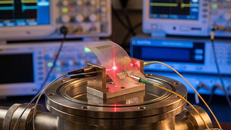
Prototype Fabrication Workflow
The fabrication of these devices is a high-precision process that bridges the gap between organic chemistry and semiconductor manufacturing.
1. Substrate Preparation: Clean the piezoelectric or flexible substrate using standard lithography cleaning protocols (Acetone, IPA, and DI water).
2. Nanoribbon Deposition: This is the most critical step. Based on the research, the 7-atom width is essential. You must use bottom-up synthesis, likely through surface-assisted polymerization of precursor molecules on a metal substrate (such as Silver or Gold). This ensures the hydrogen-terminated edges (7aGNRsH) are uniform.
3. Transfer Process: Once the nanoribbons are synthesized on their growth substrate, they must be transferred onto the target flexible/piezoelectric substrate using a polymer-assisted transfer method (e.g., PMMA transfer).
4. Electrode Patterning: Use Electron Beam Lithography (EBL) to define the contact points for the nanoribbons. Given the nanometer scale of the ribbons, standard photolithography will be too coarse.
5. Metallization: Deposit the gold or palladium contacts via thermal evaporation to establish electrical connections for testing.
6. Integration of Strain Mechanism: Mount the device onto the bending stage or connect the piezoelectric substrate to a voltage source to enable controlled mechanical deformation.
Testing and Validation Protocol
To verify that the prototype matches the theoretical predictions, follow this testing sequence:
1. Baseline Conductivity Test: Measure the electrical resistance of the unstrained 7aGNRsH device. According to the research, this should be nonconductive.
2. Strain-Conductivity Mapping: Apply incremental strain (starting from 0.1% and moving toward 3%) while measuring the electrical conductivity. You are looking for the transition from non-conductive to conductive as predicted.
3. Spectral Response Analysis: While maintaining a constant strain, expose the device to varying IR wavelengths. Use the FTIR to monitor the current output. For the 7aGNRsH-2B variant, look for the large conductivity peaks in the IR spectrum mentioned in the research.
4. Berry Curvature Verification (Advanced): If the lab has access to advanced spectroscopic tools, attempt to observe the localization of fermions near the Gamma point under strain, which confirms the underlying quantum mechanical mechanism.
Engineering Assumptions and Constraints
Because the source material is based on first-principles calculations, several engineering assumptions must be made during prototyping:
1. Dimensions: The research assumes a specific 7-atom width. In a real-world lab, we assume that any deviation from this width (e.g., 6 or 8 atoms) will significantly shift the conductivity peaks and the strain-response threshold.
2. Strain Levels: The research does not specify the exact Newtons of force required. We assume a strain range of 0.5% to 5% is the operational window for most flexible substrates.
3. Doping Concentration: For the 7aGNRsH-2B variant, we assume the boron atoms are distributed uniformly along the edges. In practice, boron doping concentrations will likely vary, which will affect the IR peak intensity.
4. Temperature: The calculations are likely at 0K or room temperature. We assume the device will operate at room temperature (approx. 298K), but thermal noise may affect the sensitivity of the IR peaks.
Technical Risks and Mitigation
1. Synthesis Precision: The biggest risk is the inability to achieve the exact 7-atom width. If the ribbons are too wide or too narrow, the strain-induced conductivity transition may not occur at the expected energy levels. Mitigation: Use high-resolution Scanning Tunneling Microscopy (STM) to verify ribbon width post-synthesis.
2. Mechanical Fatigue: Repeatedly applying strain to a flexible substrate can lead to micro-cracks in the graphene nanoribbons. Mitigation: Limit the strain amplitude and use high-quality, fatigue-resistant piezoelectric materials.
3. Contact Resistance: At the nanoscale, the resistance at the metal-graphene interface can overwhelm the signal from the nanoribbon itself. Mitigation: Use Palladium contacts and optimize the annealing temperature to ensure a low-resistance ohmic contact.
4. Signal-to-Noise Ratio: The transition from non-conductive to conductive might be subtle in a noisy lab environment. Mitigation: Use lock-in amplification techniques during electrical measurements to isolate the strain-induced signal.
Evaluate Our Quality
Serious about B2B integration? Test our premium Pulsed Electrical Resistive Carbon Heating turbostratic graphene in your lab. 100g sample packs available now.