Practical Guide: Enhancing Photonic Bandwidth: A Guide to Integrating Graphene Oxide on SiN Waveguides for Supercontinuum Generation
Introduction
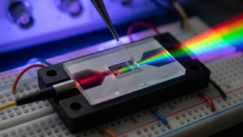
In the field of integrated photonics, supercontinuum generation (SCG) is a critical process used to convert narrow-band laser light into a broad, continuous spectrum of colors. This capability is essential for applications ranging from high-resolution spectroscopy and optical coherence tomography to advanced LIDAR systems. While silicon nitride (Si3N4) waveguides are a standard platform due to their low loss and wide transparency window, they often lack the extreme nonlinearity required to produce a very wide spectral bandwidth without using extremely high power.
Recent research has demonstrated that by incorporating a two-dimensional (2D) film of graphene oxide (GO) directly onto the waveguide, the spectral broadening can be significantly enhanced. This guide provides a practical engineering roadmap for prototyping a hybrid SiN-GO waveguide designed to boost spectral bandwidth by up to 2.4 times compared to standard SiN devices.
The Core Concept: Why Graphene Oxide
The primary limitation of standard silicon nitride waveguides in SCG is their relatively low nonlinear refractive index. Graphene oxide, despite being an insulator, possesses significant nonlinear optical properties due to its unique electronic structure.
By applying a thin film of GO onto the surface of a SiN waveguide, you create a hybrid platform. The light traveling through the SiN core interacts with the GO film via the evanescent field. This interaction introduces additional nonlinear effects that drive much more efficient spectral broadening. The key advantage of using GO over pure graphene is the ease of processing; GO can be applied via liquid-phase coating, avoiding the complex and often damaging transfer processes required for pure graphene.
Required Materials and Equipment
To prototype this device, you will need the following components and tools:
1. Photonic Integrated Circuit (PIC) Substrate: Silicon nitride (Si3N4) waveguides embedded in a silicon dioxide (SiO2) cladding layer.
2. Graphene Oxide (GO) Dispersion: A high-quality aqueous or solvent-based GO suspension.
3. Deposition System: A precision spin coater for layer-by-layer coating.
4. Lithography and Etching Tools: A mask aligner and reactive ion etcher (RIE) to create windows in the silica cladding.
5. Optical Characterization Tools: A femtosecond pulsed laser source (capable of >1000 W peak power) and an Optical Spectrum Analyzer (OSA).
6. Cleaning Agents: Isopropanol (IPA), deionized (DI) water, and oxygen plasma cleaner.
Prototype Construction Steps
The following steps outline the fabrication of a hybrid SiN-GO waveguide.
Step 1: Substrate Preparation and Windowing
The SiN waveguides must be covered by a silica (SiO2) cladding to prevent environmental contamination and manage mode confinement. However, to allow the GO to interact with the light, you must create windows in the cladding.
- Use photolithography to define rectangular windows directly over the SiN waveguide cores.
- Use Reactive Ion Etching (RIE) to remove the SiO2 in these specific windowed regions, exposing the SiN surface while leaving the rest of the chip protected.
Step 2: Surface Cleaning
Before coating, the exposed SiN surfaces must be pristine.
- Perform a rigorous cleaning cycle using IPA and DI water.
- Use an oxygen plasma clean for 2-5 minutes to remove any residual organic contaminants from the etched windows.
Step 3: Layer-by-Layer GO Coating
This is the transfer-free method described in the research.
- Deposit a controlled volume of the GO dispersion onto the windowed areas of the chip.
- Use a spin coater to spread the GO. The thickness of the film is determined by the concentration of the GO and the spin speed.
- Repeat the deposition and drying steps to build the film thickness layer by layer until the desired optical properties are achieved.
Step 4: Thermal Annealing
- Bake the chip in a controlled oven to remove remaining solvents and stabilize the GO film.
Testing and Characterization Plan
To validate the performance of your hybrid device, follow this test protocol:
1. Baseline Measurement: Measure the spectral output of the original SiN waveguide (without GO) using the femtosecond laser and the OSA. Note the initial spectral bandwidth.
2. Hybrid Measurement: Repeat the measurement with the GO-coated waveguide.
3. Bandwidth Comparison: Calculate the Full Width at Half Maximum (FWHM) of the resulting spectra. A successful prototype should show a significant increase in bandwidth, ideally approaching the 2.4x improvement noted in recent studies.
4. Power Threshold Test: Gradually increase the input peak power to determine the threshold at which the supercontinuum generation becomes efficient.
Engineering Assumptions and Starting Parameters
Because the specific fabrication parameters (concentration, speed, and dimensions) are not standardized in the source, the following values are proposed as cautious starting points for a lab-scale prototype.
- GO Dispersion Concentration: Start with 0.5 mg/mL. Higher concentrations may lead to excessive scattering losses, while lower concentrations may not provide enough nonlinearity.
- Spin Coating Speed: Start at 3000 RPM for 60 seconds. This is a standard starting point for achieving thin, uniform films.
- Window Dimensions: Aim for windows that are 50 to 200 micrometers in length, covering the most nonlinear region of the waveguide.
- Peak Power Requirement: To observe the effect, the input pulse must reach peak powers exceeding 1000 W.
Critical Risks and Mitigation
1. Film Non-uniformity: If the GO film thickness varies across the window, it will cause inconsistent nonlinear responses and potentially increase scattering losses.
- Mitigation: Use a high-precision spin coater and ensure the substrate is perfectly level.
2. Optical Loss: Excessive GO thickness or poor adhesion can lead to significant scattering and absorption losses, which can negate the benefits of the increased nonlinearity.
- Mitigation: Perform thickness characterization (e.g., via ellipsometry) before full-scale testing and optimize the number of coating layers.
3. Thermal Damage: High peak powers can cause localized heating in the GO film, potentially degrading the material.
- Mitigation: Use a low repetition rate laser to allow for thermal relaxation between pulses during initial testing.
Source Basis
This guide is based on the research findings of David J. Moss regarding supercontinuum generation in 2D graphene oxide film coated SiN waveguides. The reported 2.4x improvement in spectral bandwidth and the use of a transfer-free, windowed-cladding method are taken directly from the source. All specific fabrication parameters (RPM, concentration, window size) are engineering assumptions provided for practical implementation.
Evaluate Our Quality
Serious about B2B integration? Test our premium Pulsed Electrical Resistive Carbon Heating turbostratic graphene in your lab. 100g sample packs available now.