Breaking the Terahertz Barrier: A New Mathematical Blueprint for Graphene Absorbers
Imagine a world where medical imaging is as fast as taking a photograph, or where your smartphone communicates with satellite networks at speeds that make current fiber optics look slow. This future depends on the Terahertz spectrum, a range of electromagnetic waves that sit between the microwave signals used by your Wi-Fi and the infrared light used by remote controls. For years, scientists have struggled to control these waves perfectly, especially for high-speed communication and precision sensing. Graphene, a single layer of carbon atoms, has emerged as the perfect candidate to manipulate these waves because it is incredibly thin and its electrical properties can be changed with a simple voltage. However, designing devices with graphene has historically been a process of expensive trial and error. A recent breakthrough has changed that, providing a mathematical shortcut to designing the next generation of high-performance graphene technology.
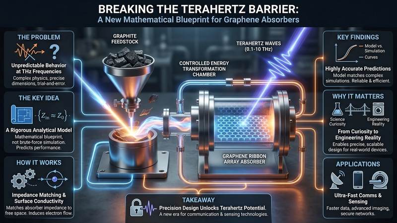
The Problem This Research Is Solving
In the pursuit of advanced Terahertz technology, engineers face a significant roadblock: the unpredictability of materials at extremely high frequencies. When working with Terahertz waves, the physical behavior of materials becomes incredibly complex. For graphene-based absorbers, which are designed to capture and dissipate these waves rather than reflecting them, the design requires extreme precision. If the dimensions of the graphene structure are off by even a tiny fraction, the device fails to absorb the target frequency.
Historically, scientists have relied on numerical simulations to solve this problem. These simulations are essentially brute-force mathematical calculations that use supercomputers to predict how a wave will interact with a specific structure. While accurate, numerical simulations are a major bottleneck in the research and development process. They are computationally expensive, taking a long time to run, and they act as a black box. A simulation might tell a researcher that a specific ribbon width works, but it does not explain the underlying physical relationship between that width and the absorption efficiency. This lack of a rigorous analytical model means that engineers cannot easily predict how changing one variable, such as the width of a graphene ribbon or the gap between ribbons, will affect the overall bandwidth. This makes the design process slow, inefficient, and highly dependent on massive computing power, preventing the rapid deployment of graphene-based components in commercial products.
The Key Idea in Plain English
The breakthrough presented by Mohammadreza Khorshidi, Shadi Daghighazar, and Reza Ghazizadeh is the creation of a rigorous analytical model. Instead of relying on a computer to guess and check millions of different combinations through brute force, the researchers developed a mathematical blueprint. This model provides a direct, algebraic way to calculate how a graphene-based absorber will perform before it is ever built.
Think of it like the difference between a chef who tries a thousand random combinations of ingredients to see which one tastes best, versus a chef who follows a precise chemical formula to achieve a specific flavor. The researchers have provided the formula. By using this analytical model, designers can extract the key parameters needed to build an absorber and then plug them into a modified design framework. This framework acts as a systematic instruction manual for constructing a device that can absorb a wide range of frequencies, rather than just one narrow frequency. This shift from trial-and-error simulation to predictable mathematical design is a fundamental leap forward for the field of nano-electronics.
How the Graphene-Based System Works
To understand why this model is so revolutionary, we must look at the physics of how graphene interacts with electromagnetic waves. Graphene is a two-dimensional material, meaning it is essentially a flat sheet of atoms. When a Terahertz wave hits a graphene surface, the electric field of the wave induces a flow of electrons within the graphene. This flow is known as surface conductivity.
The efficiency of an absorber depends on a concept called impedance matching. For a device to absorb a wave perfectly, the electrical impedance of the absorber must match the impedance of free space. If they are matched, the wave enters the material instead of bouncing off the surface. If they are mismatched, the wave is reflected. In this research, the team focused on using an array of one-layer graphene ribbons. Instead of a continuous sheet, the graphene is patterned into tiny, parallel strips.
This geometric patterning is crucial for achieving broadband performance. When the waves encounter these ribbons, the gaps between the ribbons create a specific type of electrical resonance. The width of each ribbon and the distance between them act as tuning knobs. The width of the ribbon influences the inductance of the system, while the gaps between the ribbons influence the capacitance. By balancing these two electrical properties, the researchers can ensure that the total impedance of the graphene array remains matched to free space across a wide range of frequencies.
Furthermore, the conductivity of graphene plays a vital role in energy dissipation. When the electron flow occurs within the ribbons, the energy from the Terahertz wave is converted into a tiny amount of heat through resistive losses. This is the essence of absorption. The analytical model developed by Khorshidi, Daghighazar, and Ghazizadeh allows engineers to precisely calculate exactly how wide those ribbons need to be and how much space must be between them to ensure this absorption remains consistent from 0.65 to 1.44 THz.
What the Researchers Found
The researchers tested their new analytical model by comparing its predictions against complex numerical simulations. If the math holds up against the brute-force computer models, the model is considered valid. The results were highly successful. The analytical model's predictions for absorption performance were remarkably accurate when compared to the numerical data, confirming that the mathematical framework is a reliable substitute for expensive simulations.
The performance of the designed absorber was particularly impressive. By following their new design procedure, the team created a graphene ribbon array that achieved more than 90% absorption across a very broad frequency range. Specifically, the device maintained this high efficiency from 0.65 to 1.44 THz. In the world of Terahertz technology, a bandwidth of 76% is considered exceptionally wide. Most traditional absorbers are narrow-band, meaning they only work at one specific frequency. A broadband absorber like this one is much more useful for real-world technology, where signals can fluctuate or where multiple signals need to be processed simultaneously.
The research also accounted for fabrication tolerances. In real-world manufacturing, it is impossible to make every ribbon perfectly identical. There will always be slight variations in width or spacing due to the limits of lithography and chemical deposition. The researchers' model successfully accounted for these potential errors, proving that the design is robust enough to work even when manufacturing is not perfect.
Why the Result Matters
This research is significant because it moves graphene technology from the realm of "scientific curiosity" into the realm of "engineering reality." For a technology to be used in consumer electronics, it must be predictable and scalable. You cannot build a global communication network if every single component requires a week of supercomputer simulation to design. By providing a mathematical model, this work allows for the rapid prototyping of devices.
The ability to create broadband absorbers has immediate implications for the next generation of wireless communication, such as 6G. As we move toward higher frequencies, the ability to manage signal reflections and manage bandwidth becomes critical. A device that can absorb a wide swath of the Terahertz spectrum can help prevent signal interference and improve the efficiency of signal routing in high-speed networks.
Additionally, the precision offered by this model is a game-changer for Terahertz sensing. Terahertz waves are excellent for non-destructive testing and medical imaging because they can penetrate many materials without being ionizing (meaning they are safer than X-rays). High-performance absorbers are needed to calibrate sensors and to create highly sensitive detection arrays. The more accurately we can design these components, the more precise our medical and security sensors become.
Limitations and What Still Needs Testing
While this research is a major step forward, it is important to recognize that we are still in the foundational stages of graphene integration. The study focuses on an analytical model and a theoretical design framework; it does not represent a finished commercial product.
One of the primary challenges remains the physical fabrication of these nanostructures at a massive scale. While the model accounts for some fabrication tolerances, producing perfectly uniform graphene ribbons over large areas using industrial processes is still a complex and expensive endeavor. There is also the issue of material purity. The model assumes certain levels of graphene conductivity, but in a real-world manufacturing environment, impurities, defects in the graphene lattice, or residues from the chemical processes used to make the ribbons can alter the conductivity and degrade performance.
Future research will need to bridge the gap between this mathematical model and the realities of industrial mass production. We need to see how these designs hold up when manufactured using large-scale chemical vapor deposition (CVD) on flexible substrates or other common industrial materials. Additionally, testing the device's stability over time—ensuring that the graphene does not degrade or react with the environment—will be essential before these absorbers can be integrated into consumer devices.
Real-World Applications
The implications of this research extend far beyond the laboratory. In the field of security, Terahertz absorbers can be used in advanced scanners at airports or border crossings. These scanners can look through clothing and packaging to identify threats without the harmful effects of ionizing radiation. A broadband absorber allows these scanners to operate more efficiently across a wider range of materials.
In the medical sector, Terahertz technology is being explored for skin cancer detection and dental imaging. Because Terahertz waves are sensitive to water content in human tissue, they can help doctors distinguish between healthy and diseased cells. The precision design provided by this research allows for the creation of highly sensitive, specialized sensors that could eventually be used in handheld diagnostic tools.
In the realm of communications, as we look toward the 6G era, the demand for high-frequency signal management will be unprecedented. Graphene-based components could be integrated into antennas and signal processors to manage the intense flow of data. The ability to design these components with mathematical certainty ensures that the infrastructure for the next generation of the internet is built on a foundation of reliable, high-performance hardware.
If You Remember One Thing
If there is one takeaway from this research, it is that mathematical models are the bridge between theoretical physics and practical engineering. By moving away from trial-and-error simulations and toward a rigorous analytical framework, researchers have unlocked a way to design highly efficient, broadband graphene devices with unprecedented precision.
FAQ
What exactly is Terahertz radiation?
Terahertz radiation refers to a specific part of the electromagnetic spectrum that exists between microwaves and infrared light. It is characterized by waves that are much shorter than microwaves but much longer than visible light. Because of its unique properties, it can pass through many non-conductive materials like paper, plastic, and clothing, making it incredibly useful for sensing and imaging.
Why is graphene considered the ideal material for this technology?
Graphene is a single layer of carbon atoms that possesses extraordinary electrical and mechanical properties. Because it is a two-dimensional material, its surface conductivity is highly sensitive to external influences, which allows for incredibly fine control over electromagnetic waves. This tunability is much harder to achieve with traditional bulk metals, making graphene uniquely suited for high-frequency applications.
How does a ribbon-shaped structure help in absorbing waves?
When an electromagnetic wave hits a continuous sheet, it interacts with the material uniformly. However, by breaking the graphene into a pattern of ribbons, we create a series of tiny resonators. These ribbons create a specific electrical response involving both inductance and capacitance. By tuning the width and the spacing of these ribbons, we can match the impedance of the graphene to the impedance of free space, which allows the device to capture and dissipate the wave's energy rather than reflecting it.
Why is a mathematical model better than a computer simulation?
Numerical simulations are like a "black box" where you input numbers and wait for a computer to spit out a result. They are very slow and require massive amounts of computing power. A mathematical model, on the other hand, is a direct formula. It allows researchers to see exactly how changing a design parameter affects the final result, making the design process much faster, more intuitive, and more efficient.
Can this technology be used in my smartphone anytime soon?
While this research is a significant breakthrough, it is still in the research and development phase. Moving from a mathematical model and a laboratory prototype to a mass-produced component in a smartphone requires solving many manufacturing challenges. We must ensure that graphene can be produced cheaply and consistently at scale, and that these components can be integrated into existing electronic manufacturing workflows.
Conclusion
The work by Mohammadreza Khorshidi, Shadi Daghighazar, and Reza Ghazizadeh provides a vital piece of the puzzle in the quest for advanced Terahertz technologies. By replacing slow, complex simulations with a rigorous analytical model, they have created a way to design broadband graphene absorbers with high precision and efficiency. While challenges in manufacturing and material purity remain, the ability to mathematically predict and control the behavior of graphene ribbons marks a turning point. This research brings us one step closer to a future of ultra-fast communications and non-invasive sensing, driven by the incredible potential of two-dimensional materials.
Evaluate Our Quality
Serious about B2B integration? Test our premium Pulsed Electrical Resistive Carbon Heating turbostratic graphene in your lab. 100g sample packs available now.