Mastering the Invisible: How Graphene and Carbon Nanotube Hybrids Shield Modern Electronics
Every modern electronic device, from the smartphone in your pocket to the medical sensors inside a hospital, operates by sending and receiving electromagnetic signals. While these signals are essential for communication, they also create a hidden environmental hazard known as electromagnetic interference. When these waves leak from one device and collide with another, they cause signal noise, data errors, and even complete device failure. Historically, the industry has relied on heavy, bulky metal enclosures to act as shields. However, as we move toward an era of ultra-lightweight wearables and compact biomedical implants, these heavy metal boxes are no longer viable. We need a new class of materials: thin, lightweight, and incredibly efficient shields that can stop invisible waves without adding significant weight.
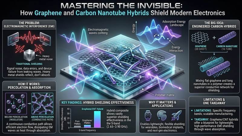
The Problem This Research Is Solving
The core challenge addressed by this investigation is the growing density of electromagnetic noise in our technological environment. As we pack more electronic components into smaller spaces, the risk of cross-talk and interference increases exponentially. Traditional shielding methods often rely on reflection, where a metal surface bounces the electromagnetic waves away. While effective, reflection can actually cause more problems by bouncing the interference around a room or a device casing, potentially creating new areas of high-intensity noise. Furthermore, heavy metal shielding is incompatible with the modern push for lightweight, flexible, and biocompatible electronics.
To tackle this, a team of researchers including Anita Grozdanov, Perica Paunović, Iva Dimitrievska, Andrea Petanova, Duska Kleut, and Svetlana Jovanović investigated a more sophisticated approach. They sought to create polymer-based nanocomposites that do not just reflect these waves, but actually absorb them. By integrating carbon-based nanostructures into a polymer matrix, the goal was to develop a material that turns electromagnetic energy into harmless thermal energy through a dense, conductive internal network. This research focuses on optimizing the structure of these materials by comparing different methods of treating graphene to see which creates the most effective shield for the S-band frequency range, which is critical for various wireless communication technologies.
The Key Idea in Plain English
The researchers decided to move away from the simple idea of just mixing graphene into plastic. Instead, they explored two more advanced strategies. The first was metal decoration, where tiny particles of silver are attached to the surface of the graphene to boost its electrical conductivity. The second, and more successful, was the creation of a hybrid carbon network. This involves mixing graphene—which is a flat, two-dimensional sheet—with carbon nanotubes, which are long, one-dimensional tubes.
Think of graphene as flat sheets of paper and carbon nanotubes as long, thin straws. If you just have sheets of paper, they stack on top of each other but leave large gaps. If you add the straws, they bridge those gaps, creating a much more interconnected and complex three-dimensional web. To make this web even stronger, the researchers used e-beam irradiation, a process that uses high-energy electrons to modify the structure of the material. This irradiation helps create a better "glue" between the carbon structures and the plastic, ensuring that the electrical network is seamless and the material can effectively trap and destroy electromagnetic waves.
How the Graphene-Based System Works
To understand why these hybrid structures work so well, we must look at the physics of conductivity and percolation. In a polymer composite, the plastic itself is an insulator, meaning it does not conduct electricity. For a material to shield against electromagnetic interference, it must have a continuous, unbroken path of conductive material that allows electrons to move freely throughout the structure. This is known as the percolation threshold. Once enough conductive filler is added to form this continuous network, the electrical properties of the composite change drastically.
In the graphene/PMMA (polymethyl methacrylate) system, the graphene sheets provide large surface areas for interaction. When carbon nanotubes are added to the mix, they act as bridges that connect graphene sheets that might otherwise be separated by layers of insulating polymer. This hybrid morphology—combining 2D and 1D structures—creates a much more efficient labyrinth for electromagnetic waves.
The researchers specifically focused on the mechanism of absorption. When an electromagnetic wave enters this dense, interconnected network, it induces an oscillating current in the conductive carbon structures. Because the network is so complex and full of microscopic "obstacles," these electrons are forced to move in jagged, unpredictable paths. This resistance to movement causes the kinetic energy of the moving electrons to be converted into heat. This is the essence of absorption-dominant shielding: instead of bouncing the interference back into the environment, the material captures the energy and dissipates it as a negligible amount of heat.
Furthermore, the e-beam irradiation plays a vital role in interface engineering. By exposing the composite to high-energy electrons, the researchers can modify the chemical bonds between the PMMA polymer and the carbon fillers. This improves the adhesion at the interface, reducing the "gaps" where waves might slip through and ensuring that the mechanical and electrical properties are optimized.
What the Researchers Found
The research team utilized a suite of advanced analytical techniques to verify how these modifications affected the material. They used Scanning Electron Microscopy (SEM) to look at the physical structure, Fourier-Transform Infrared Spectroscopy (FTIR) to understand the chemical bonds, and Thermal Gravimetric Analysis (TGA) combined with Differential Scanning Calorimetry (DSC) to test how the materials behaved under heat. Finally, a Vector Network Analyzer (VNA) was used to measure the electromagnetic shielding effectiveness in the S-band (2.65–3.90 GHz).
The results provided a clear winner. The hybrid graphene/CNT (carbon nanotube) composites, especially those that had undergone 50 kGy of e-beam irradiation, outperformed the silver-decorated graphene (G/Ag) composites. Specifically, the irradiated PMMA/AH50 sample (which had a thickness of 0.28 mm) and the irradiated PMMA/AM1 sample (with a thickness of 0.48 mm) reached shielding effectiveness (SE) values between 11 and 13 dB.
Two critical trends emerged from the data. First, thickness is a major factor; as the thickness of the film increased, the shielding effectiveness increased because there was a larger volume for the electromagnetic waves to travel through, providing more opportunities for absorption. Second, the hybrid structure was superior to the metal-decorated structure. Even though silver is highly conductive, the 3D labyrinth created by the graphene/CNT hybrid was much more effective at trapping and absorbing waves via absorption rather than relying on the simple reflection provided by metal particles. The study confirmed that the combination of 2D and 1D carbon structures, enhanced by irradiation, creates the most efficient conductive network for EMI shielding.
Why the Result Matters
These findings are significant because they provide a blueprint for the next generation of lightweight, high-performance electronic shielding. By moving away from heavy metals and toward engineered carbon hybrids, we open the door to a much wider range of applications. The ability to achieve significant shielding (up to 13 dB) in a very thin, lightweight film is a game-changer for the electronics industry.
The shift from reflection-dominant to absorption-dominant shielding is particularly important for the integrity of modern wireless environments. In a world filled with Bluetooth, Wi-Fi, and 5G signals, we cannot afford to have devices simply "bouncing" interference around. We need materials that "swallow" the noise. This research demonstrates that we can achieve this through clever material architecture—specifically by using hybrid carbon structures and controlled irradiation—rather than just piling on more heavy metal. This allows for the design of thinner, lighter, and more efficient devices that can operate reliably in increasingly crowded electromagnetic environments.
Limitations and What Still Needs Testing
While these results are highly promising, it is important to note that this research is currently at the laboratory and fundamental science stage. The study demonstrates what is possible in a controlled environment, but several hurdles remain before these materials can be widely used in consumer products.
One major challenge is the scalability of the e-beam irradiation process. While irradiation is an effective way to modify polymers, integrating high-energy electron beams into a continuous manufacturing line for thin films is a complex and expensive engineering task. Additionally, the cost of high-purity graphene and carbon nanotubes remains relatively high compared to traditional metallic shielding materials.
There is also the question of long-term durability. While the researchers used TGA and DSC to look at thermal stability, more testing is needed to see how these nanocomposites behave over years of use in varying environmental conditions, such as extreme humidity, temperature fluctuations, or mechanical stress. Finally, while the S-band was tested, real-world devices operate across a vast spectrum of frequencies. Future research will need to determine if these hybrid structures maintain their high absorption efficiency across higher frequency bands, such as the millimeter-wave frequencies used in advanced 5G and 6G communications.
Real-World Applications
The potential applications for these irradiated graphene/CNT nanocomposites are vast and span multiple high-tech industries. In the consumer electronics sector, these films could be integrated into the casings of smartphones, tablets, and laptops to prevent internal component interference, allowing for even smaller and more powerful devices.
In the medical field, the lightweight and thin nature of these composites makes them ideal for shielding sensitive biomedical sensors and implants. As we move toward more sophisticated wearable health monitors and even internal neural interfaces, protecting these sensitive electronics from external electromagnetic noise is a critical safety and performance requirement.
The aerospace and satellite industries also represent a massive market. Satellites and aircraft are packed with complex electronic systems that must operate in environments with significant electromagnetic activity. Lightweight, high-performance shielding is essential to reduce the overall weight of the aircraft or spacecraft while ensuring that mission-critical electronics are protected from interference. Finally, as we enter the era of autonomous vehicles, where sensors like LiDAR and radar must operate with absolute precision, these advanced carbon-based shields could play a vital role in ensuring that the vehicle's electronic "nervous system" remains free from noise.
If You Remember One Thing
If you take away only one thing from this research, let it be this: the most effective way to stop electromagnetic interference is not by bouncing the waves away with metal, but by creating a complex, three-dimensional "trap" using a hybrid mix of graphene and carbon nanotubes, which can be further optimized through electron-beam irradiation to absorb the energy entirely.
FAQ
Question: What exactly is electromagnetic interference (EMI)?
Answer: Electromagnetic interference, or EMI, is a disturbance generated by an electric current or a magnetic field that can affect an electrical circuit by causing unwanted signals or noise. It is essentially "electronic noise" that can disrupt the communication or function of sensitive devices.
Question: Why is graphene so special for this type of work?
Answer: Graphene is a single layer of carbon atoms arranged in a hexagonal lattice. It has extraordinary electrical conductivity and a massive surface area relative to its size. This makes it an ideal material for creating the conductive networks needed to interact with and absorb electromagnetic waves.
Question: How does irradiation help the material?
Answer: Using an e-beam (electron beam) to irradiate the polymer helps to create a more cohesive and stable connection between the graphene flakes and the plastic matrix. This process can modify the molecular structure of the polymer, improving the electrical pathways and the overall mechanical strength of the composite.
Question: What is the difference between reflection and absorption in shielding?
Answer: Reflection is when a shield, like a metal plate, bounces the electromagnetic waves away from the device. Absorption is when the shield captures the wave's energy and converts it into a tiny amount of heat. Absorption is generally preferred because it doesn't create "bounced" noise that can interfere with other devices nearby.
Question: What is PMMA, and why is it used?
Answer: PMMA, or polymethyl methacrylate, is a common transparent thermoplastic often known by trade names like Plexiglass. It is used here as the "matrix" or host material. It is chosen because it is easy to work with and can act as a stable carrier for the carbon nanostructures.
Conclusion
This research marks a significant step forward in the development of advanced functional materials. By moving beyond simple mixtures and exploring the synergistic effects of graphene, carbon nanotubes, and e-beam irradiation, the researchers have demonstrated a way to create highly efficient, absorption-dominant electromagnetic shields. As the world becomes increasingly crowded with electronic signals, the ability to create lightweight, thin, and highly effective shielding through engineered carbon architectures will be essential for the next generation of technology, from the smartphones in our hands to the life-saving medical devices of the future.
Evaluate Our Quality
Serious about B2B integration? Test our premium Pulsed Electrical Resistive Carbon Heating turbostratic graphene in your lab. 100g sample packs available now.