A van der Waals Lock: Directional, Defect-Free Carbon-Nanotube Interconnects by Elastically Induced Form-Locking in Perforated Graphene
As the world pushes the boundaries of how small and fast electronic devices can become, we are running into a fundamental wall. For decades, silicon has been the king of the computer chip, but it is reaching its physical limits. As transistors shrink, the tiny copper wires that connect them—the interconnects—become a major bottleneck. They get too hot, they leak too much electricity, and they simply cannot carry current as efficiently as we need them to. This has led scientists to look toward carbon nanotubes as the ultimate successor. These tiny, hollow cylinders of carbon are incredible conductors, capable of carrying massive amounts of electricity with almost no resistance. However, there is a massive catch. It is remarkably difficult to plug a carbon nanotube into a circuit without ruining the very properties that make it useful. If you connect it using traditional methods, you often end up damaging the nanotube itself, turning a perfect highway for electrons into a cluttered obstacle course of atomic defects.
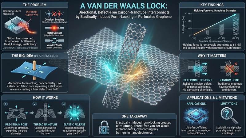
The Problem This Research Is Solving
The central challenge in nanoelectronics is the contact problem. To make a functioning circuit, a carbon nanotube must be physically and electrically connected to something else, such as a metal wire or another layer of material. Currently, researchers are stuck between three equally difficult options, each with a fatal flaw.
The first method involves covalent functionalization. This is essentially a chemical approach where the atoms of the nanotube are chemically bonded to the contact point. While this creates a very strong mechanical connection, it comes at a high cost to conductivity. In a perfect carbon nanotube, the carbon atoms are arranged in a specific way called sp2 hybridization, where the atoms form a flat, hexagonal lattice. This structure allows electrons to flow smoothly across the tube. When you create a covalent bond to secure the tube, you force the carbon atoms into a different configuration known as sp3 hybridization. This change shifts the geometry from a flat plane to a tetrahedral shape. To an electron traveling through the tube, this change in geometry looks like a massive roadblock or a scattering defect. These defects cause the electrons to bounce back or lose energy, significantly increasing the electrical resistance and defeating the purpose of using the nanotube in the first place.
The second method is the van der Waals side-contact. This method avoids chemical bonding altogether, instead relying on the natural, weak attraction between surfaces known as van der Waals forces. Because no chemical bonds are broken, the nanotube's lattice remains perfect, and the electrical conductivity stays incredibly high. However, these connections are mechanically fragile. Because the bond is so weak, the nanotube can easily slide out of its socket, making the device unstable and unreliable for long-term use.
The third method is in-situ growth, where the nanotubes are grown directly on the circuit during manufacturing. This sounds like the perfect solution, but it requires extremely high temperatures, often exceeding 700 degrees Celsius, to get the carbon atoms to arrange themselves into tubes. Standard semiconductor manufacturing processes, known as CMOS processing, use materials that would melt or warp under such intense heat. This makes in-situ growth fundamentally incompatible with the way we currently build microchips.
The Key Idea in Plain English
The research led by Meik Klein proposes a fourth way that avoids the traps of chemistry, weakness, and heat. The idea is to use physics instead of chemistry to create a "mechanical lock." Imagine a piece of thin, stretchy fabric with a tiny hole in it. If you take a small stick and push it through that hole, then pull the fabric tight, the hole will squeeze the stick. If the fabric is elastic, it will want to return to its original shape, and that squeezing force will hold the stick firmly in place without you ever needing to use glue or welding.
In this microscopic version, the fabric is a single layer of graphene, and the stick is a carbon nanotube. Instead of using chemicals to glue the nanotube in place, we use the natural elastic tension of the graphene to "clamp" the tube. By pre-stretching the graphene before the nanotube is inserted, we create a state of tension. Once the tube is in place and the tension is released, the graphene acts like a tiny, high-strength clamp. This provides a strong mechanical hold through pure physical force, while the carbon atoms in the nanotube remain completely untouched, preserving their ability to conduct electricity perfectly.
How the Graphene-Based System Works
To understand how this works at the atomic level, we have to look at the mechanics of the graphene membrane. The process begins with a graphene sheet that has been precisely perforated to create a pore. The diameter of this pore is slightly smaller than the diameter of the carbon nanotube. Because graphene is incredibly strong yet highly flexible, it can be stretched significantly without breaking.
Through a process called pre-straining, the graphene is pulled slightly to expand the pore, making it large enough for the nanotube to pass through. Once the nanotube is threaded through the hole, the tension is released. The graphene seeks to return to its original, relaxed state, which causes the edges of the pore to contract inward toward the center of the tube. This creates a radial clamp. The tube is now held in place by the elastic restoring force of the graphene.
This is not just a static grip; it is a dynamic interaction. The stability of the connection is determined by the balance of forces between the carbon atoms of the nanotube and the carbon atoms of the graphene. As the nanotube tries to move, the atoms in the pore rim push back. Because this is a purely mechanical interaction, there is no permanent change to the atomic structure of either material. The electrons see nothing but a continuous, perfect lattice, allowing them to zip through the connection as if no joint existed at all.
What the Researchers Found
Using advanced molecular-dynamics simulations, the team mapped out how these systems behave under different conditions. They tested a variety of nanotube sizes, specifically looking at armchair-shaped tubes with diameters ranging from very small (5,5) to much larger (20,20). They also tested different levels of tension, or strain, applied to the graphene.
The results were highly revealing. First, the team found that the holding force—the amount of force required to pull the tube out—is remarkably strong. It can reach up to 61 nano-newtons, and they discovered that this strength scales linearly with the circumference of the tube. Essentially, the larger the tube, the more surface area is available for the graphene to grip, and the stronger the connection becomes.
Second, the researchers discovered a very interesting phenomenon regarding the amount of tension applied. One might assume that more tension would always lead to a stronger grip, but the simulations showed a counterintuitive optimum. The strongest, most stable connection occurs when the graphene is only slightly strained, specifically between 0.5% and 1%. If you pull the graphene too hard, you actually make the connection less effective. This happens because excessive strain pushes the atoms in the pore rim too close together. At these extremely short distances, the atoms enter the Pauli-repulsive branch of the Lennard-Jones potential. This is a state where the electron clouds of the atoms overlap and push back violently. This intense repulsion actually softens the overall carbon-carbon bonds in the graphene, making the structure less stable and reducing the effective holding force.
Finally, the researchers found that the system acts like a "mechanical diode." When you try to pull the tube out one way, it is much harder than when you pull it the other way. This is because the force of the pull causes the graphene membrane to buckle and deform, creating a "finger-trap" effect. The membrane forms a small funnel shape around the tube, which allows the tube to slide in easily but creates a physical barrier that resists being pulled back out. This directional anisotropy is a powerful feature, as it allows for the creation of components that only allow movement or signal in one direction.
Why the Result Matters
This discovery is significant because it offers a deterministic way to build nanoscale joints. In traditional manufacturing, creating a connection often involves a degree of randomness—some connections might be stronger than others depending on how the chemicals react. This new method is based on the predictable, mathematical laws of elasticity. If you know the diameter of the tube and the strain applied to the graphene, you can predict exactly how strong the connection will be.
Furthermore, because this method is "chemistry-free," it solves the fundamental conflict between mechanical strength and electrical performance. We no longer have to choose between a strong connection that ruins the electricity or a good conductor that falls apart. By using the elastic energy stored in the graphene, we get both. This represents a new class of "defect-free" interconnects that could be vital for the next generation of ultra-high-speed computing.
Limitations and What Still Needs Testing
It is important to note that this research is currently based on computer simulations. While these simulations are highly sophisticated and use realistic models of atomic interaction, they are not a substitute for physical reality. There are several significant hurdles that must be overcome before this can be used in a factory.
The first is the fabrication of the pores. The research requires pores that are smaller than 3 nanometers in diameter, located precisely in a single layer of graphene. Creating such tiny, consistent holes in a material that is only one atom thick is a monumental engineering challenge. The second challenge is the insertion process. Getting a single carbon nanotube to thread through a sub-3-nanometer hole is like trying to thread a needle with a microscopic thread while wearing oven mitts. Scientists may need to use techniques like dielectrophoresis—using electric fields to guide the tube—to achieve this. Finally, the research needs to be moved from the virtual world of simulations into a physical laboratory to prove that these forces hold up in real-world conditions.
Real-World Applications
If the engineering challenges can be solved, the applications for this technology are vast. In the realm of post-silicon electronics, these "van der Waals locks" could serve as the primary interconnects for future computer processors, allowing for much higher clock speeds and lower power consumption.
Beyond computer chips, this technology has exciting potential in Micro-Electro-Mechanical Systems (MEMS). In these tiny machines, many components need to move or act as one-way valves. The "mechanical diode" effect discovered by the researchers could be used to create nanoscale valves or protective mechanisms that prevent damage from mechanical overload.
Perhaps most interestingly, the researchers suggest that this could lead to the creation of gradient-index (GRIN) micro-optics. By creating arrays of carbon nanotubes with varying densities, they can create a material that bends light in a controlled, predictable way. This could lead to incredibly small, high-performance lenses and light-steering components for advanced imaging and communication technologies.
If You Remember One Thing
If you take away only one concept from this research, let it be this: the future of nanoelectronics may not depend on new chemicals, but on clever uses of mechanical tension to create strong, perfect, and defect-free electrical connections.
FAQ
How does a carbon nanotube actually conduct electricity?
Carbon nanotubes are made of carbon atoms arranged in a seamless cylinder. Because of their unique atomic structure, they have a high density of "delocalized" electrons. These are electrons that aren't stuck to any single atom but are free to move throughout the entire tube, allowing them to carry electrical current with very little resistance.
Why does adding chemicals to a nanotube ruin it?
When you use chemicals to bond a nanotube to a wire, you change the hybridization of the carbon atoms from sp2 to sp3. In an sp2 state, the atoms are flat and provide a smooth path for electrons. In an sp3 state, the atoms are arranged in a three-dimensional shape that acts like a physical obstacle, causing electrons to scatter and lose energy.
What is graphene, and why is it useful here?
Graphene is a single layer of carbon atoms arranged in a hexagonal lattice. It is one of the strongest and most flexible materials known to science. In this research, it is used as the "clamp" because it is strong enough to hold the nanotube but flexible enough to be stretched and then snap back into shape.
What does "mechanical diode" mean?
A diode in electronics is a component that allows current to flow in only one direction. A mechanical diode works the same way but for movement. Because the graphene membrane buckles and forms a funnel shape around the nanotube, it allows the tube to slide in one way easily, but it resists being pulled out the other way.
Is this technology ready to be used in smartphones?
No, not yet. This research is in the computational modeling stage. While the simulations are very promising, scientists still need to figure out how to manufacture these tiny pores and how to physically insert the nanotubes into them in a real-world factory setting.
Conclusion
The search for the perfect replacement for silicon is one of the most important quests in modern science. As we have seen, the problem is not just finding a better conductor, but finding a better way to connect it. The work by Meik Klein and his colleagues provides a brilliant solution: using the inherent elasticity of graphene to create a mechanical lock. By moving away from damaging chemical bonds and embracing the predictable physics of molecular tension, we are opening a door to a new era of defect-free, high-performance nanoscale technology.
Evaluate Our Quality
Serious about B2B integration? Test our premium Pulsed Electrical Resistive Carbon Heating turbostratic graphene in your lab. 100g sample packs available now.