Practical Guide: Building Ultra-Fast Radiation Detectors: A Guide to Graphene-Optimized Silicon Carbide PIN Detectors
The Challenge of Extreme Radiation Environments
In high-energy physics, space exploration, and nuclear monitoring, standard silicon-based detectors face a fundamental problem: radiation damage. When exposed to intense X-ray or particle flux, the crystal lattice of a standard silicon detector undergoes displacement damage, leading to increased leakage current and degraded signal timing. This degradation makes it difficult to distinguish between individual particle events in high-rate environments.
For engineers designing sensors for satellite electronics or nuclear reactor safety systems, the goal is to find a substrate that is inherently radiation-hard and a contact architecture that can maintain ultra-fast signal collection even after significant exposure. Recent research has identified a powerful combination: 4H-Silicon Carbide (SiC) optimized with a graphene electrode layer. This hybrid approach offers a path toward detectors that maintain sub-100 picosecond timing resolution even after being subjected to mega-gray levels of radiation.
The Graphene-SiC Advantage
The research by Jiang et al. demonstrates that adding a graphene layer to a silicon carbide PIN detector provides two critical benefits. First, it significantly improves the time resolution. While standard 4H-SiC PIN detectors are already fast, the graphene-optimized version showed a nearly 40 percent improvement in timing resolution, reaching approximately 58 picoseconds.
Second, the graphene layer acts as an incredibly stable electrode that maintains high charge collection efficiency (CCE). Even after 1 MGy of X-ray irradiation, the detector maintained a CCE of 99.24 percent. For an engineer, this means the sensor does not need frequent recalibration or replacement when operating in high-flux environments. The graphene layer ensures that the electrical contact remains stable and that the charge carriers are collected with minimal dispersion.
Primary Application: High-Speed Particle Timing in Extreme Flux
The most practical application for this technology is in high-speed particle timing for high-energy physics experiments or space-based cosmic ray detectors. In these scenarios, the detector must distinguish between particles arriving in incredibly rapid succession. A time resolution of 58 picoseconds allows for much higher "event rates" before the signals overlap and become indistinguishable.
If you are building a prototype for a small lab or a startup focusing on radiation-hardened sensors, this technology is ideal for:
1. Space-based cosmic ray monitoring where radiation doses are high and maintenance is impossible.
2. Nuclear reactor monitoring where real-time, high-speed particle flux data is required for safety.
3. High-energy physics experiments where timing precision is critical for vertex reconstruction.
Required Materials and Equipment
To prototype a graphene-optimized SiC detector, you will need specialized materials and cleanroom-grade equipment. Since this is a specialized semiconductor process, small labs should look for contract research organizations (CROs) to handle the fabrication if they lack an in-house cleanroom.
Materials:
1. 4H-SiC Substrate: High-purity silicon carbide wafers.
2. Graphene: High-quality, large-area CVD-grown graphene.
3. Contact Metals: Gold (Au) and Nickel (Ni) for the top and bottom electrodes.
4. Photoresist: Positive or negative resist for lithography.
5. Etchants: Hydrofluoric acid (HF) for surface cleaning and specific metal etchants.
6. PMMA: Polymethyl methacrylate for the graphene transfer process.
Equipment:
1. Chemical Vapor Deposition (CVD) system (if growing graphene in-house).
2. Electron-beam evaporator or Sputter coater for metal deposition.
3. Photolithography setup (Mask aligner).
4. Scanning Electron Microscope (SEM) for surface inspection.
5. High-voltage DC power supply (capable of at least 500V).
6. Fast pulse generator and high-bandwidth oscilloscope (at least 20 GHz bandwidth) for timing tests.
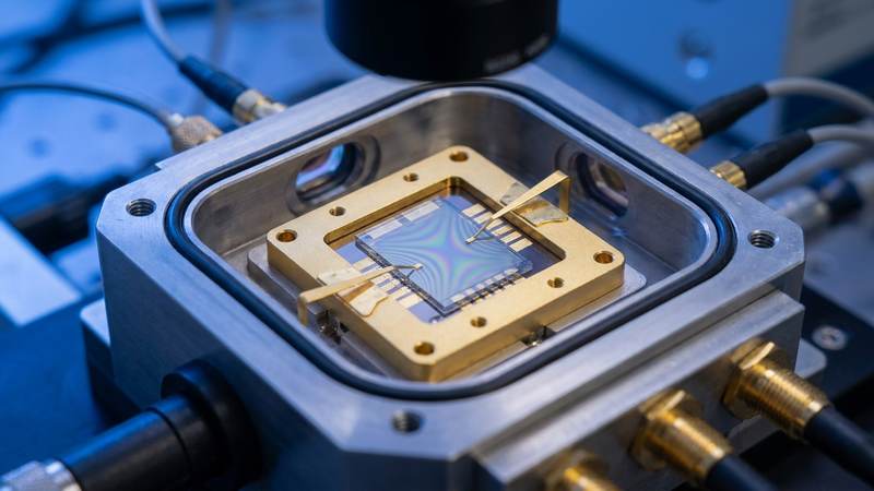
Prototype Fabrication Steps
The following steps outline the engineering process for creating a graphene-on-SiC PIN structure. Note that exact temperatures and chemical concentrations are not specified in the source research and are provided here as engineering assumptions based on standard semiconductor practices.
1. Substrate Preparation:
Begin with a 4H-SiC wafer. Perform a standard RCA cleaning process to remove organic and ionic contaminants. This typically involves an ammonium sulfide solution or a Piranha etch (H2SO4:H2O2) to ensure a pristine surface for graphene adhesion.
2. Graphene Depstrate and Transfer:
Since growing graphene directly on SiC can be difficult to control for specific electrode shapes, the most practical method is the PMMA-assisted transfer. Grow the graphene on a copper foil via CVD. Spin-coat PMMA onto the graphene, etch the copper away, and then transfer the PMMA/graphene stack onto the SiC substrate.
3. Electrode Patterning:
Use photolithography to define the electrode areas. Apply a photoresist, expose it through a mask, and develop it. This defines where the graphene will be exposed and where it will be covered.
4. Metal Deposition:
Using an electron-beam evaporator, deposit a thin layer of Nickel (Ni) followed by Gold (Au). The Nickel acts as an adhesion and ohmic contact layer, while the Gold provides a stable, non-oxidizing surface.
5. Final Cleaning and Encapsulation:
Remove the remaining PMMA using an acetone bath. For long-term stability, consider a thin layer of Al2O3 (Alumina) via Atomic Layer Deposition (ALD) to encapsulate the device, though the source research suggests the graphene itself provides significant stability.
Testing and Validation Protocol
To verify if your prototype matches the performance of the graphene-optimized SiC detector, you must follow a rigorous testing plan.
1. Leakage Current Measurement:
Apply a DC bias voltage (starting at 100V and increasing to 300V) and measure the leakage current. Based on the research, you are looking for an ultralow leakage current, ideally in the range of 10^-10 A.
2. Capacitance-Voltage (C-V) Characterization:
Perform C-V sweeps to determine the depletion voltage. The goal is to confirm full depletion at a voltage consistent with the SiC properties (the source suggests around 120V).
3. Time Resolution Testing:
This is the most critical test. Use a pulsed X-ray source or a beta-particle source (like 90Sr) and a high-bandwidth oscilloscope. Measure the time interval between the pulse trigger and the signal peak. You are aiming for a resolution in the 50-65 picosecond range.
4. Charge Collection Efficiency (CCE):
Measure the collected charge relative to the incident radiation energy. After exposure to a high-dose X-ray source (e.g., 160 keV), the CCE should remain above 99 percent.
Engineering Risks and Mitigation
Building these devices involves several high-stakes technical risks:
1. Graphene Delamination:
The interface between the graphene and the SiC substrate is sensitive. If the transfer process is not perfect, the graphene may peel or bubble. Mitigation: Ensure the SiC surface is extremely clean and optimize the annealing temperature after transfer to improve adhesion.
2. Contact Resistance:
High contact resistance at the graphene-metal interface can ruin the ultra-fast timing resolution. Mitigation: Use a heavy metal deposition (like Ni) and consider a post-deposition thermal anneal to promote better electrical contact.
3. High Voltage Arcing:
Operating at 300V on a small, micro-patterned device carries a risk of dielectric breakdown or arcing. Mitigation: Use high-quality encapsulation and ensure the device geometry is designed with sufficient spacing between electrodes.
Source Basis and Assumptions
This guide is based on the research findings of Jiang et al. (2026) regarding graphene-optimized silicon carbide PIN detectors. The performance metrics (58ps timing, 99.24% CCE, and 1 MGy tolerance) are taken directly from the research results.
Engineering assumptions made in this guide include:
- The use of the PMMA-transfer method for graphene application.
- The use of Ni/Au for metallization.
- The assumption that the user has access to high-bandwidth (20 GHz+) measurement equipment.
- The use of 160 keV X-rays as the primary testing radiation source.
Evaluate Our Quality
Serious about B2B integration? Test our premium Pulsed Electrical Resistive Carbon Heating turbostratic graphene in your lab. 100g sample packs available now.