Graphene Transistors Hit Gigahertz Speeds Through Advanced Material Engineering
Imagine a computer that operates at speeds we can barely fathom, utilizing components so thin that they are essentially two-dimensional. As our current silicon-based technology reaches its physical limits, the world of nanoelectronics is looking toward a new frontier. The challenge is no longer just making things smaller, but making them faster and more efficient without melting under the heat of their own operation. Recent breakthroughs in graphene technology suggest that we are moving closer to a future where high-frequency, high-speed electronic switching is possible through the use of hot electrons and engineered material interfaces.
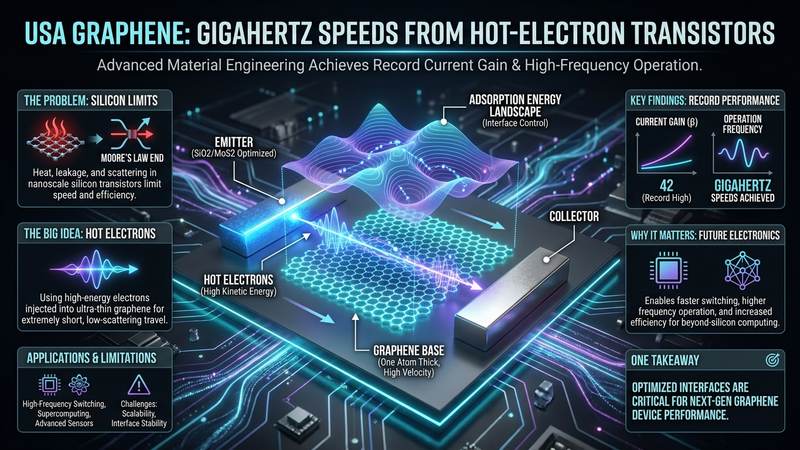
The Problem This Research Is Solving
For decades, silicon has been the king of the semiconductor industry, powering everything from smartphones to supercomputers. However, silicon is approaching a fundamental bottleneck known as the end of Moore's Law. As transistors are shrunk to the nanometer scale to increase density, they suffer from significant issues: leakage current and extreme heat generation. In a traditional transistor, electrons move through the semiconductor, but they often lose their kinetic energy through a process called scattering. When electrons collide with the atoms in the crystal lattice, they transfer their energy to those atoms, which manifests as heat.
This thermal energy is the enemy of high-speed computing. As devices get faster, they generate more heat, which in turn increases resistance and can lead to device failure. Furthermore, traditional transistors struggle to maintain high gain—the ability of a small input signal to control a large output signal—at extremely high frequencies. To reach the next level of computational power, we need a device that can handle high-energy electrons without losing all that energy to heat through scattering. We need a way to inject "hot" electrons—electrons with high kinetic energy—into a material and ensure they reach their destination before they lose their energy.
The Key Idea in Plain English
The solution lies in a specialized type of device called a Graphene-Based Hot-Electron Transistor, or GHET. Instead of relying on the standard movement of charge used in your laptop's processor, these transistors use the energy of the electrons themselves. The core idea is to inject electrons into a single layer of graphene with significant extra energy, making them "hot." Because graphene is incredibly thin—only one atom thick—the path the electron must travel is extremely short. This reduces the chances of the electron bumping into something and losing its energy.
The breakthrough described in this research involves a technique called material engineering at the emitter-base junction. The emitter is the part of the device that injects the electrons, and the base is the graphene layer they travel through. By carefully choosing and optimizing the materials used for the emitter, researchers can control exactly how these hot electrons enter the graphene. If the connection between the emitter and the base is perfect, the electrons enter with the right energy and momentum to fly through the graphene without hitting anything. This optimization is what allows the device to achieve high gain and high speeds, effectively solving the heat and efficiency problems that plague traditional semiconductors.
How the Graphene-Based System Works
To understand how this system functions, we must look at the architecture of the transistor. A transistor typically consists of three parts: the emitter, the base, and the collector. In a GHET, the base is a sheet of graphene. Graphene is a unique material because its electrons behave like massless particles, allowing them to move at incredibly high velocities.
The researchers focused on the emitter-base (E/B) composition. The emitter is the component that supplies the hot electrons. In this study, they experimented with different materials for the emitter, specifically silicon dioxide (SiO2) and molybdenum disulfide (MoS2). When a voltage is applied, electrons are pushed from the emitter into the graphene base. Because these electrons are injected with energy higher than the Fermi level of the graphene, they are considered "hot."
The performance of the transistor depends heavily on how these electrons transition from the emitter into the graphene. If there is a mismatch in the energy levels or the physical structure of the interface, the electrons will scatter. This scattering is a devastating effect; it causes the electrons to lose their "hot" status and turns their kinetic energy into heat. By engineering the interface—essentially smoothing the way for the electrons—the researchers reduced these scattering losses. This allows more electrons to pass through the base successfully to the collector, which increases the current gain and allows the device to operate at much higher frequencies.
What the Researchers Found
The findings presented by C. Strobel, André Heinzig, André Hiess, Martin Knaut, Md Tarik Hossain, Andrey Turchanin, Tilo Meister, Frank Ellinger, Jens Trommer, Viktor Havel, and Thomas Mikolajick demonstrate a major leap in performance. The researchers discovered that the composition of the emitter-base junction is the most critical factor in determining how well the device works.
First, they achieved a record-high common-emitter current gain, denoted as beta, of 42 using a SiO2/Gr structure. Current gain is a vital metric; it represents how much the device amplifies the input signal. A beta of 42 in a graphene-based device is exceptionally high, proving that graphene can indeed act as an efficient switching material.
Second, when they swapped the SiO2 for MoS2, they observed a dramatic increase in the maximum output current. The MoS2/Gr structure produced a current density of approximately 2000 A/cm2. This is a massive number in the world of nanoelectronics, representing a significant improvement over previous graphene transistors. High current density is essential for creating devices that can drive larger loads and operate in more demanding environments.
Finally, the researchers were able to determine the cutoff frequencies for these devices. The cutoff frequency is the speed limit of the transistor—the point at which it can no longer effectively amplify a signal. For their nonoptimized SiO2/Gr devices, they achieved cutoff frequencies close to 1 GHz. This moves the technology out of the realm of theoretical physics and into the realm of practical, high-speed electronics.
Why the Result Matters
These results are significant because they address the two main pillars of high-speed electronics: speed and efficiency. In the past, graphene transistors were often criticized for having very low gain or being unable to operate at high frequencies due to the inherent difficulty of injecting hot electrons efficiently. This research proves that those limitations are not fundamental to the material itself, but rather to how the device is constructed.
By showing that we can achieve a gain of 42 and gigahertz operation, this research provides a roadmap for creating a new class of high-frequency transistors. This has massive implications for the future of telecommunications, where we need faster and more efficient ways to process signals for 6G and beyond. It also opens doors for high-speed signal processing in aerospace and advanced computing architectures. The ability to achieve high current densities using MoS2 suggests that we can create devices that are not only fast but also capable of handling significant power, which is a requirement for many real-world electronic systems.
Limitations and What Still Needs Testing
While these results are groundbreaking, it is important to maintain a realistic perspective. This research represents a laboratory-scale achievement. The devices described were created in a highly controlled research environment, and they are not yet ready for mass production in a consumer device like a smartphone.
Several hurdles remain. First is the issue of scalability. While we can engineer a single, perfect emitter-base junction in a lab, doing this consistently across a billion transistors on a single silicon wafer is an immense manufacturing challenge. Second is material integration. Integrating graphene and MoS2 into existing CMOS (Complementary Metal-Oxide-Semiconductor) manufacturing processes requires extreme precision to avoid contamination and defects.
Finally, thermal management in a practical setting still needs testing. While the researchers succeeded in reducing scattering-induced heat within the device, a real-world chip will contain billions of these components. Understanding how these GHETs behave in a dense, high-power environment is a necessary next step before this technology can move from the lab to the factory.
Real-World Applications
The potential applications for high-speed, high-gain graphene transistors are vast. One of the most immediate areas is high-frequency communication. As we move toward much higher frequency bands for wireless data, such as Terahertz communications, traditional silicon-based components will struggle to keep up. GHETs could provide the necessary speed to handle these massive data rates.
Another application is in the realm of ultra-fast signal processing. In radar systems, satellite communications, and high-speed networking, the ability to amplify and switch signals at gigahertz or even terahertz speeds is critical. The high current density and high gain found in this research make graphene transistors ideal candidates for these high-performance roles.
Furthermore, as we look toward the future of neuromorphic computing—computers designed to mimic the human brain—the ability to create extremely small, efficient, and fast switches is vital. The low-power, high-speed nature of hot-electron transistors could allow for much more efficient neural networks implemented on a chip, potentially revolutionizing how artificial intelligence is processed at the hardware level.
If You Remember One Thing
If you take away only one piece of information from this research, let it be this: Graphene is no longer just a theoretical curiosity; through precise material engineering of the emitter-base junction, we can finally harness the power of hot electrons to create transistors that are both incredibly fast and highly efficient.
FAQ
What exactly is a hot electron?
A hot electron is an electron that possesses much more kinetic energy than the average electron in a material. In electronics, we want these electrons to travel through a device to carry a signal. The goal is to keep them "hot" long enough to do their job before they lose their energy to heat.
Why is graphene used as the base material?
Graphene is an ideal base because it is incredibly thin, essentially a two-dimensional sheet of carbon atoms. Because it is so thin, an electron traveling through it has a much lower chance of hitting an atom and losing its energy through scattering. This makes it much more efficient for high-speed applications.
What does "current gain" actually mean?
Current gain, often called beta, is a measure of how well a transistor can turn a small input signal into a larger output signal. A higher gain means the transistor is more effective at amplifying electricity. Achieving a gain of 42 is a major milestone for graphene-based devices.
Why is "gigahertz" frequency important?
Frequency refers to how many times a transistor can switch on and off per second. One gigahertz means one billion times per second. The higher the frequency, the faster the device can process information. To support modern high-speed internet and communications, we need transistors that can operate at these extremely high speeds.
What is the role of MoS2 in this research?
Molybdenum disulfide, or MoS2, is a two-dimensional semiconductor. In this research, it was used as part of the emitter-base junction to see if it could improve the device's performance. The researchers found that using MoS2 allowed for much higher current densities than other materials, which is essential for high-performance electronics.
Conclusion
The research conducted by the team, including C. Strobel, André Heinzig, André Hiess, Martin Knaut, Md Tarik Hossain, Andrey Turchanin, Tilo Meister, Frank Ellinger, Jens Trommer, Viktor Havel, and Thomas Mikolajick, marks a pivotal moment in the evolution of nanoelectronics. By mastering the engineering of the emitter-base interface, they have unlocked the ability to utilize hot electrons in graphene, achieving unprecedented levels of gain and frequency. While the road from the laboratory to the commercial market is filled with manufacturing and integration challenges, the proof of concept provided here is a resounding success. This work paves the way for a new generation of high-speed, high-efficiency electronics that could eventually redefine the limits of computing and communication.
Evaluate Our Quality
Serious about B2B integration? Test our premium Pulsed Electrical Resistive Carbon Heating turbostratic graphene in your lab. 100g sample packs available now.