Practical Guide: Precision Graphene Engineering: Fabricating Sub-10nm GNR FETs via AC-AFM Lithography
The GNR Fabrication Challenge
For engineers working in next-generation nanoelectronics, graphene nanoribbons (GNRs) represent a critical frontier. Unlike bulk graphene, which lacks a natural band-gap, GNRs allow for size-dependent band-gap engineering. This means that by controlling the width of the ribbon, we can tune its electrical properties, making it a viable candidate for field-effect transistors (FETs) in ultra-miniaturized logic circuits.
However, the industry faces a massive bottleneck in fabrication. Traditional methods like electron-beam lithography (EBL) or photolithography (PL) are the industry standards but come with significant drawbacks for small-scale prototyping. EBL is prohibitively expensive and requires massive capital investment in cleanroom facilities. PL lacks the resolution required for sub-10nm features. Furthermore, these methods often introduce chemical contaminants or structural defects during the resist stripping and etching phases, which degrade the exceptional electrical and thermal properties that make graphene desirable in the first place.
To move from theoretical research to functional nano-devices, we need a method that is low-cost, high-resolution, and contamination-free. This guide explores the implementation of direct-write electrochemical AFM lithography to solve these issues.
The Solution: AC-AFM Electrochemical Lithography
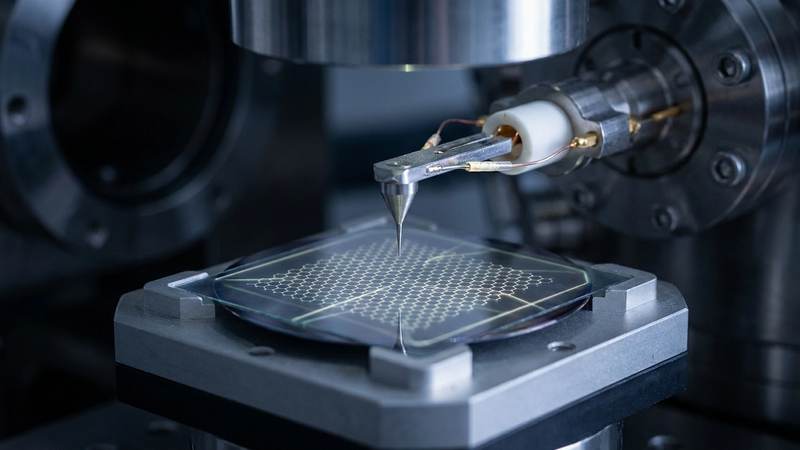
The research presented by Liu and Durkan offers a paradigm shift: using an Atomic Force Microscope (AFM) as a direct-write lithography tool. Instead of using light or electron beams to expose a resist, this method uses an AFM tip as a mobile, nanoscale electrode.
By applying an alternating current (AC) bias between the AFM tip and the graphene substrate within an electrochemical environment, we can induce localized electrochemical reactions. This allows us to "write" or etch patterns directly into the graphene. Because the AFM tip can be positioned with sub-nanometer precision, we can create GNRs with widths below 10nm.
The primary advantages for a startup or small lab are:
1. Resolution: Achieving feature sizes below 10nm, which is difficult for standard lithography.
2. Cleanliness: The process is contamination-free as it avoids polymer resists.
3. In situ capability: You can modify or characterize the device in the same environment where it was fabricated.
4. Cost: It utilizes standard AFM equipment rather than multi-million dollar EBL systems.
Required Laboratory Setup and Materials
To replicate or test this approach, your lab will need specific instrumentation and high-quality precursors.
Equipment:
1. AFM with AC Bias Capability: This is the most critical component. Standard AFMs only provide DC bias. You require an AFM system capable of applying an alternating current (AC) to the probe tip.
2. High-Resolution AFM Probes: Conductive tips are required to act as the moving electrode.
3. Semiconductor Probe Station: For post-fabrication electrical characterization.
4. Microfluidic Cell or Environmental Chamber: To hold the electrolyte in a controlled, minimal volume over the sample.
Materials:
1. Graphene-on-Insulator Substrate: Typically, a monolayer of graphene transferred onto a silicon substrate with a thin layer of silicon dioxide (SiO2) (e.g., 285nm or 90nm SiO2) to act as the bottom gate dielectric.
2. Electrolyte Solution: The source does not specify the exact chemical composition. For prototyping, a cautious starting range would be a dilute aqueous solution of a mild electrolyte, such as 0.1M KOH or a similar salt solution, depending on the desired etching rate.
3. Deionized (DI) Water: For rinsing and cleaning.
4. Nitrogen Gas: For drying the sample.
Experimental Procedure for GNR FET Fabrication
Since the source is a research paper, the exact operational parameters (voltage, frequency, and concentration) are not explicitly detailed for a general user. The following steps are an engineering projection based on the research principles.
Step 1: Substrate Preparation
Clean your graphene-on-insulator substrate using standard methods (e.g., RCA cleaning or UV-Ozone treatment) to ensure no organic contaminants are present. The graphene must be high quality to observe the band-gap effects.
Step 2: Electrolyte Application
Apply a very thin, controlled layer of the electrolyte over the graphene surface. This can be done using a micro-pipette or a controlled humidity chamber. The liquid layer must be thin enough to allow the AFM tip to maintain contact without excessive hydrodynamic drag, but thick enough to facilitate the electrochemical reaction.
Step 3: Patterning via AC-AFM
Mount the sample in the AFM. Set the AFM to a contact or near-contact mode.
Apply the AC bias.
Engineering Assumption: Based on similar electrochemical AFM studies, a starting voltage range of 1V to 5V (peak-to-peak) and a frequency range of 100 Hz to 10 kHz is recommended.
Program the AFM to follow a specific path to etch the graphene. The width of the ribbon will be determined by the scan speed, the AC amplitude, and the tip radius. To achieve sub-10nm widths, the scan speed must be extremely slow and the voltage kept at the lower end of the assumption range to prevent over-etching.
Step 4: Rinsing and Drying
Once the pattern is written, immediately rinse the sample with DI water to stop the electrochemical reaction. Use a gentle stream of nitrogen gas to dry the sample to prevent water spots or salt residue from forming on the graphene.
Step 5: Contact Deposition
Since this method avoids the need for electrodes during the patterning phase, you must now deposit metal contacts (such as Gold or Palladium) using a standard shadow mask or EBL to connect the GNR channel to your testing equipment.
Testing and Characterization Plan
Once the GNR FET is fabricated, you must verify that the etching was successful and that the band-gap has been correctly engineered.
1. Topography Mapping: Use the AFM in tapping mode (without bias) to confirm the physical dimensions of the etched ribbons. Verify that the width is indeed below the 10nm target.
2. Electrical Characterization (I-V Curves): Use a semiconductor probe station to measure the Drain-to-Source Current (Id) as a function of Gate Voltage (Vg).
3. Band-gap Verification: If the GNR is narrow enough, you should observe a clear modulation of the current (an "on-off" ratio) as the gate voltage sweeps through the Fermi level. A successful fabrication will show a significant decrease in current at the charge neutrality point, indicating the presence of a band-gap.
4. Mobility Calculation: Use the slope of the I-d/V-g curve in the linear regime to calculate the carrier mobility. This will tell you if the electrochemical process introduced too many defects.
Engineering Assumptions and Risk Mitigation
Because this is an emerging technique, several variables must be managed carefully.
Assumptions:
- Electrolyte Concentration: We assume a dilute solution is sufficient. High concentrations may lead to uncontrolled etching and loss of resolution.
- AC Parameters: We assume low voltage and moderate frequency. High voltages may cause tip damage or substrate breakdown.
- Tip Geometry: We assume a standard conductive AFM tip is sufficient, though specialized nano-tips may be required for sub-5nm precision.
Risks and Mitigation:
- Tip Degradation: The electrochemical reaction can coat the tip with reaction byproducts. Mitigation: Regularly check tip sharpness and replace probes if resolution degrades.
- Over-etching: The most significant risk is the "widening" of the ribbon beyond the target width. Mitigation: Start with very low AC amplitudes and increase incrementally.
- Substrate Damage: Excessive voltage can cause electrolysis of the water, creating gas bubbles that can lift the graphene. Mitigation: Use extremely thin liquid films and low-frequency AC.
By following this guide, labs can begin exploring the potential of GNR-based electronics without the massive overhead of traditional lithography, enabling faster prototyping of next-generation nano-devices.
Evaluate Our Quality
Serious about B2B integration? Test our premium Pulsed Electrical Resistive Carbon Heating turbostratic graphene in your lab. 100g sample packs available now.