Deciphering the Chaos: How Mathematical Decomposition Unlocks the Secrets of Graphene Growth
Imagine you are looking at a vast, crowded ballroom through a heavily frosted glass window. You can see that people are moving and that there are distinct groups of individuals, but you cannot clearly identify who is standing where or how many people are in each group because their silhouettes overlap and blur together. This is exactly the dilemma faced by scientists studying the next generation of electronic materials. Graphene, a single layer of carbon atoms arranged in a hexagonal lattice, is famous for its extraordinary properties, such as incredibly high electron mobility and transparency. However, when engineers try to grow graphene on a substrate like silicon carbide to create real-world transistors, the material is rarely perfect. It comes in different thicknesses, has structural defects, and follows the uneven terrain of the underlying surface. To understand how to use this material, we need to see its electronic structure with perfect clarity, but the tools we use often provide a blurry, blended mess of information.
The Problem This Research Is Solving
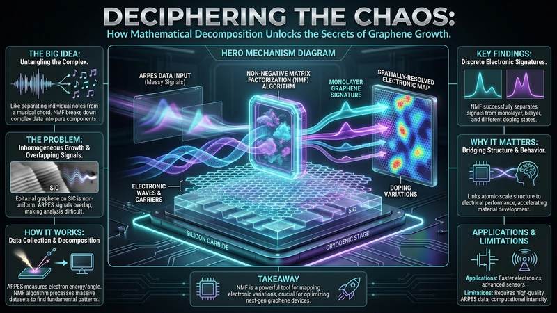
The primary tool used to study the electronic behavior of materials is Angle-Resolved Photoemission Spectroscopy, or ARPES. This technique works by shining high-energy light on a sample, which knocks electrons out of the material. By measuring the energy and the angle at which these electrons escape, scientists can map out the electronic band structure, which tells us exactly how electrons will move through the material. In a perfect, uniform sample, this is straightforward. However, real-world epitaxial graphene grown on silicon carbide is notoriously inhomogeneous. This means that the electronic properties change depending on where you look on the surface.
When a sample is inhomogeneous, the ARPES signal becomes a composite of many different electronic states. For instance, one area might contain a single layer of graphene, while a nearby area contains two layers, and a third area might sit right on the edge of an atomic step in the substrate. The detector receives a mixture of all these signals simultaneously. Because these electronic states often overlap in energy and momentum, it becomes incredibly difficult to distinguish the unique signature of a single layer from that of a bilayer or a defective region. Traditional analysis methods often rely on complex mathematical models that require researchers to guess what the components might look like beforehand, which can introduce human bias and fail to capture unexpected electronic variations that the researchers did not anticipate.
The Key Idea in Plain English
To overcome this confusion, researchers Masaki Imamura and Kazutoshi Takahashi have turned to a sophisticated mathematical technique known as Non-negative Matrix Factorization, or NMF. To understand NMF, think about a complex musical chord played on a piano. A chord is a single sound that you hear, but it is actually composed of several distinct notes being played at once. If you had a magical mathematical tool that could take that single chord and tell you exactly which notes were played and how loudly each one was struck, you would have a powerful way to analyze music.
NMF works similarly for scientific data. In the case of ARPES, the "chord" is the messy, overlapping spectrum collected by the detector, and the "notes" are the pure electronic signatures of the different graphene layers or surface features. The crucial part of NMF is the "non-negative" constraint. In the physical world, you cannot have a negative number of electrons or a negative amount of light intensity. By forcing the mathematical algorithm to only use positive numbers, the decomposition becomes much more physically meaningful. Unlike other methods that might suggest a component has a negative intensity to make the math work, NMF ensures that every part of the final result corresponds to something that could actually exist in a laboratory. This allows the algorithm to find the underlying, pure patterns in the data without the researchers needing to tell the computer what to look for in advance.
How the Graphene-Based System Works
The specific system used to demonstrate this power is epitaxial graphene grown on silicon carbide (SiC). This growth process is a marvel of chemical engineering. Instead of simply laying graphene on top of a surface, scientists use heat to induce the sublimation of silicon. When silicon carbide is heated to extremely high temperatures in a vacuum, the silicon atoms on the surface detach and evaporate away, leaving behind the carbon atoms. These remaining carbon atoms naturally organize themselves into a hexagonal lattice, forming graphene.
However, this process is not perfectly uniform. The surface of silicon carbide is not a flat plane; it consists of tiny, microscopic terraces separated by atomic-scale steps. As the carbon atoms rearrange themselves, they follow the contours of these steps. This leads to a variety of local environments. You might have a single layer of graphene that is chemically bonded to the substrate in a way that prevents it from conducting electricity effectively, often called a buffer layer. You might then have a true monolayer of graphene on top of that, or perhaps a second layer that has grown on top of the first. Each of these configurations—the buffer layer, the monolayer, the bilayer, and the transition zones at the step edges—produces a slightly different electronic signature. The way the electrons move is dictated by the local arrangement of atoms and the electrostatic environment created by the substrate, meaning the electronic structure is a direct reflection of the physical topography and chemical composition of the surface.
What the Researchers Found
By applying the NMF framework to spatially-resolved ARPES data, Imamura and Takahashi were able to untangle this complex web of signals. The algorithm successfully decomposed the massive, messy datasets into a set of discrete, physically interpretable spectral components. These components represented the "pure" electronic signatures of the different graphene states present on the surface. For example, the NMF could clearly separate the signature of a monolayer from that of a bilayer, even when they were located right next to each other.
Beyond just identifying the different layers, the researchers were able to create spatial heatmaps by looking at the activation matrix. This is a mathematical map that shows how much of each pure spectral component is present at every specific coordinate on the sample's surface. These heatmaps turned out to be incredibly intuitive. They allowed the researchers to visualize the distribution of different graphene thicknesses and to see exactly how the electronic properties changed as they crossed an atomic step edge. This meant they could quantitatively map the transition from a monolayer to a bilayer and correlate those changes directly with the physical features of the silicon carbide substrate. The NMF approach proved it could take a massive, complex dataset and turn it into a clear, visual map of electronic inhomogeneity.
Why the Result Matters
This capability is a significant leap forward for materials science because it bridges the gap between what we see under a microscope and how the material actually behaves electrically. In the development of high-performance electronics, uniformity is everything. For a transistor to work predictably, the electrical properties of the graphene channel must be consistent across the entire device. If a designer knows that certain growth conditions lead to unexpected bilayer formation or electronic shifts at step edges, they can adjust the manufacturing process to mitigate these effects.
Furthermore, this research provides a way to validate growth models. If a theoretical model predicts that a certain temperature should produce a specific distribution of layers, scientists can now use NMF to check if that prediction holds true in a real sample. This ability to quantify and map electronic variations allows for much tighter control over the properties of low-dimensional materials, moving us closer to a world where graphene-based components can be manufactured with the same precision as current silicon-based technology.
Limitations and What Still Needs Testing
While the NMF framework is a powerful tool, it is important to understand its role. NMF is a data analysis technique, not a fabrication method. It can tell you exactly what is wrong with your sample, but it cannot fix the sample itself. It provides a way to see the inhomogeneity, but the underlying cause—the atomic steps or the uneven sublimation of silicon—remains a physical challenge that must be solved through better growth techniques.
Additionally, the complexity of the algorithm increases significantly as the datasets grow larger and more complex. While the researchers have demonstrated its efficacy, applying this to even larger, more multidimensional datasets will require significant computational resources. There is also the question of whether NMF can distinguish between even more subtle variations, such as those caused by single point defects or dopants, which might produce spectral changes that are even more minute than those caused by layer thickness changes.
Real-World Applications
The implications for real-world technology are vast. In the realm of high-frequency electronics, graphene is a prime candidate for use in transistors that operate much faster than current silicon technology. By using NMF to ensure the electronic homogeneity of graphene on SiC, manufacturers can create more stable and predictable high-speed communication components, which are essential for the rollout of 6G and beyond.
Beyond transistors, graphene's unique properties make it ideal for advanced sensors and optoelectronics. Highly sensitive chemical or biological sensors rely on the fact that any molecule landing on the graphene surface will change its electrical conductivity. To make these sensors commercially viable, the baseline conductivity of the graphene must be perfectly uniform. NMF provides the analytical rigor needed to ensure that the sensor's response is due to the target molecule and not just a variation in the graphene's local thickness. Finally, in the emerging field of quantum computing, where even a single defect can ruin a quantum state, the ability to precisely map and manage electronic environments is vital for the development of stable quantum architectures.
If You Remember One Thing
If you remember only one thing from this research, let it be this: scientific progress often relies on finding better ways to see through the noise, and by using clever mathematics to untangle the messy reality of material surfaces, we can unlock the true potential of the next generation of electronic materials.
FAQ
What exactly is ARPES and why is it so important for graphene research?
Angle-Resolved Photoemission Spectroscopy is a technique that uses light to eject electrons from a material. By measuring the energy and the angle of these ejected electrons, scientists can determine the electronic band structure, which is essentially the "roadmap" that shows how electrons move through the material. This is crucial for graphene because its electrical conductivity is determined by this very structure.
Why is silicon carbide used as a substrate for growing graphene?
Silicon carbide is a widely used substrate because it can be thermally decomposed to produce graphene. When heated, the silicon atoms leave the surface, leaving behind a thin, self-assembled layer of carbon atoms that form the graphene lattice. This process, known as epitaxial growth, allows for the creation of high-quality graphene that is chemically integrated with the substrate.
How does NMF differ from other ways of analyzing scientific data?
Most traditional ways of analyzing data require researchers to make assumptions about what the underlying components look like before they start the math. This can lead to biased results if the researcher's assumptions are wrong. NMF is different because it does not require these prior assumptions; it simply looks for the most statistically probable components that are physically possible, meaning it can discover unexpected features in the data.
Why is inhomogeneity a problem for graphene-based devices?
Inhomogeneity means that the material's properties, like its thickness or its electronic structure, change from one spot to another. For electronic components like transistors, this is a major problem because it leads to unpredictable performance. If the material is not uniform, the device may not work the same way every time it is turned on, making it unreliable for precision electronics.
Is this research going to lead to graphene-powered smartphones immediately?
Not directly. This research is fundamental science aimed at understanding and characterizing materials at a highly granular level. While it provides the tools necessary to improve graphene manufacturing, there are still many engineering and economic hurdles to overcome before graphene-based components are found in everyday consumer electronics.
Conclusion
The work conducted by Masaki Imamura and Kazutoshi Takahashi represents a significant step forward in our ability to master the complexities of two-dimensional materials. By providing a robust, mathematical way to decompose and visualize the electronic landscapes of epitaxial graphene, they have given scientists a powerful lens to see through the chaos of inhomogeneous surfaces. As we continue to refine our ability to map and control these materials, the transition from laboratory curiosity to industrial standard for next-generation electronics becomes increasingly possible.
Evaluate Our Quality
Serious about B2B integration? Test our premium Pulsed Electrical Resistive Carbon Heating turbostratic graphene in your lab. 100g sample packs available now.