Practical Guide: Building a High-Sensitivity Terahertz Detector Using Graphene Josephson Junctions
Introduction
The terahertz (THz) frequency band represents a significant gap in modern sensing technology. While microwave and infrared detectors are mature and commercially available, the THz regime—situated between these two spectrums—lacks a standardized, highly sensitive quantum sensor. This gap is critical for applications in security scanning, high-speed communications, and deep-space spectroscopy.
Recent research has identified graphene-based Josephson Junctions (JJs) as a premier candidate for solving this problem. Unlike traditional semiconductor detectors, graphene offers frequency-independent absorption and extremely low electronic heat capacity. This allows the device to respond almost instantly to radiation-induced heating. This guide outlines how a research lab or a specialized hardware startup can approach prototyping a THz detector based on the principles of gate-tunable photoresponse in graphene JJs.
The Engineering Concept
The device operates on a principle known as radiation-induced electron heating. In a Josephson Junction, two superconductors are separated by a thin barrier—in this case, a layer of graphene. At cryogenic temperatures, a specific amount of current, known as the critical current (Ic), can flow through the junction without any voltage being produced.
When THz radiation hits the graphene junction, the photons are absorbed, raising the temperature of the electron gas within the graphene. This increase in electron temperature causes a rapid suppression of the critical current. By applying a constant DC bias current just below the critical current, this suppression causes a sudden, measurable voltage (Vph) to appear across the junction. This voltage is the signal.
The unique advantage here is gate tunability. By applying a voltage to a nearby gate electrode, you can tune the carrier density in the graphene. This allows you to adjust the critical current to a specific operating point, potentially enabling the device to detect single photons of THz radiation.
Required Materials and Hardware
Building this prototype requires specialized laboratory equipment. This is not a benchtop electronics project; it is a cryogenic physics engineering project.
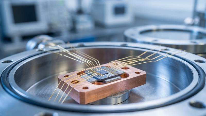
1. Graphene Heterostructure: High-quality, encapsulated graphene is required. The standard architecture is a stack consisting of a substrate (such as Si/SiO2), a layer of hexagonal Boron Nitride (hBN) for encapsulation, a monolayer of graphene, and a top layer of hBN.
2. Superconducting Electrodes: Niobium (Nb) or Aluminum (Al) are the standard choices for the superconducting leads. Niobium is preferred for its higher critical temperature, which provides more operational headroom.
3. Fabrication Tools: An Electron-Beam Lithography (EBL) system and a shadow evaporation system (for the superconducting leads) are necessary to create the micron-scale junctions.
4. Cryogenic Environment: A Helium-3 (He-3) cryostat or a Dilution Refrigerator is required. The research indicates optimal operation at 1.7 K, though single-photon sensitivity may require temperatures in the millikelvin (mK) range.
5. Measurement Electronics:
- A high-precision DC voltage source for the bias current.
- A low-noise DC voltage source for the gate electrode.
- A high-impedance, low-noise pre-amplifier to capture the photovoltage.
- A THz source (such as a mercury vapor lamp with a monochromator or a THz frequency multiplier chain) for testing.
Prototype Assembly Steps
Step 1: Device Fabrication
The most critical step is the fabrication of the Josephson Junction. Using EBL, define the geometry of the superconducting leads. The gap between the leads must be small enough to allow for the Josephson effect but large enough to prevent electrical shorts. Use shadow evaporation to deposit the superconducting material (e.g., Niobium) over the graphene layer. The graphene must be encapsulated in hBN to protect it from environmental noise and ensure high carrier mobility.
Step 2: Cryogenic Mounting
Mount the fabricated chip onto a high-thermal-conductivity substrate (like oxygen-free high-conductivity copper) within the cryostat. Ensure that the electrical leads are thermally anchored to the cryostat stages to prevent heat leaks from the room-temperature electronics from reaching the device.
Step 3: Electrical Characterization
Before applying THz radiation, perform a baseline characterization. Apply a DC bias and sweep the current to map the I-V (current-voltage) characteristics. Identify the critical current (Ic) where the voltage first appears. This is your baseline.
Step 4: Gate Tuning
Apply a gate voltage to the device. Monitor how the critical current changes as a function of the gate voltage. You are looking for the regime where the junction shows hysteretic I-V characteristics, as this is where the device becomes most sensitive to small thermal fluctuations.
Step 5: THz Illumination and Signal Capture
Introduce THz radiation into the cryostat, ideally through a specialized window (such as a polyethylene or diamond window) that is transparent to THz frequencies. Measure the resulting photovoltage (Vph) as you vary the intensity of the THz source.
Testing and Characterization Plan
To validate the prototype, you must calculate two primary metrics: Responsivity and Noise-Equivalent Power (NEP).
1. Responsivity (R): This is the ratio of the generated photovoltage to the absorbed power (Vph / P). Based on the research, a successful prototype should aim for a responsivity in the range of 88 kV W^-1. To measure this, you must accurately determine the power (P) absorbed by the graphene, which often requires a calibrated THz power meter or a known attenuation setup.
2. Noise-Equivalent Power (NEP): This measures the minimum detectable power. It is calculated by dividing the intrinsic voltage noise of the device by the responsivity. The target for a high-performance sensor is in the range of 45 aW Hz^-1/2. To measure this, you must measure the voltage noise floor of the device in the absence of THz radiation.
3. Temperature Dependence: Repeat the measurements at different temperatures (e.g., 1.7 K, 1.0 K, and 0.5 K) to confirm the scaling of the photoresponse and the transition into the single-photon detection regime.
Engineering Risks and Assumptions
This project carries significant technical risks that must be managed:
Thermal Management: The device relies on electron heating, but excessive heating will destroy the superconducting state of the leads. You must assume that the thermal coupling between the electrons and the lattice is the limiting factor. If the device heats up too much, the critical current will drop to zero regardless of the THz signal.
Fabrication Complexity: The success of the device is highly dependent on the quality of the graphene-hBN interface. Any impurities or trapped bubbles during the transfer process will lead to unpredictable critical currents and noisy signals. We assume the use of professional-grade EBL and cleanroom facilities.
Signal-to-Noise Ratio (SNR): At the millikelvin temperatures required for single-photon detection, the electronic noise from your measurement cables can easily overwhelm the tiny photovoltage. We assume the use of cryogenic coaxial cables and low-noise amplifiers.
Temperature Assumptions: While the research demonstrates strong results at 1.7 K, we assume that for industrial-grade sensitivity, the user will need to operate at temperatures below 1 K to minimize thermal noise.
Source Basis: This guide is based on the experimental findings of Zhou et al. (2026) regarding the gate-tunable photoresponse of graphene Josephson Junctions. The responsivity and NEP values provided are based on their reported experimental results.
Evaluate Our Quality
Serious about B2B integration? Test our premium Pulsed Electrical Resistive Carbon Heating turbostratic graphene in your lab. 100g sample packs available now.