Engineering the Terahertz Gap: The Miniaturized Graphene Absorber
Imagine a world where security scanners can detect hidden contraband through clothing without using harmful X-rays, or where doctors can image the early stages of skin cancer with absolute precision, all using a form of light that is currently difficult to capture and control. This is the promise of terahertz radiation, a slice of the electromagnetic spectrum that sits in the gap between microwaves and infrared light. While these waves are incredibly useful because they can penetrate many non-conducting materials, they are notoriously difficult to absorb and manipulate efficiently. For years, the devices designed to capture these waves have been too bulky or too sensitive to the angle at which the light hits them. Recent work by Kayhan Çelik and his team has introduced a breakthrough in this field, designing a graphene-based metamaterial absorber that is not only incredibly small but also capable of absorbing terahertz waves from almost any direction and across a wide range of frequencies.
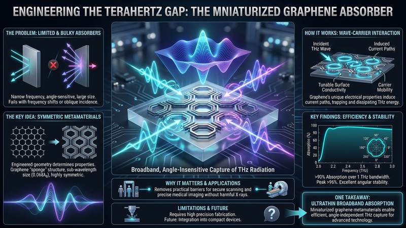
The Problem This Research Is Solving
The primary challenge in terahertz technology is the creation of an absorber that is simultaneously broadband, miniaturized, and polarization-insensitive. Most traditional absorbers are designed to work at a single, specific frequency. If the incoming wave shifts slightly in frequency, the device fails to capture it. This is a significant limitation for real-world applications where signals are rarely a single, pure tone. Furthermore, many existing designs suffer from polarization sensitivity. In electromagnetics, polarization refers to the orientation of the electric field of a wave. If an absorber is designed for vertically polarized waves, it may completely fail to capture horizontally polarized waves, meaning the device would have to be perfectly aligned with the source of the radiation to function.
Another critical hurdle is size. To interact with a wavelength of light, a structure typically needs to be a significant fraction of that wavelength in size. In the terahertz range, this often results in devices that are too large to be integrated into modern microelectronics or wearable sensors. Researchers have sought ways to shrink these components without sacrificing their ability to absorb energy. The goal is to create a system that maintains high absorption efficiency even when the device is shrunk to a fraction of the operating wavelength and when the radiation hits the surface at a steep, oblique angle.
The Key Idea in Plain English
To solve these problems, the researchers turned to metamaterials. A metamaterial is not a naturally occurring substance but an engineered structure where the geometry determines the properties of the material. By arranging graphene—a single layer of carbon atoms arranged in a honeycomb lattice—into specific, repeating patterns called unit cells, the researchers created a surface that behaves like a sponge for terahertz waves.
The core idea is to create a structure so small and so symmetric that the incoming terahertz wave does not perceive a difference in orientation. Whether the wave is tilted, flipped, or hitting the surface at a seventy-degree angle, it encounters the same geometric arrangement of graphene. By carefully tuning the size and spacing of these patterns, the researchers were able to force the terahertz waves to resonate within the structure. This resonance converts the electromagnetic energy of the wave into heat, effectively absorbing the radiation rather than reflecting it back.
How the Graphene-Based System Works
The effectiveness of this absorber lies in the interaction between graphene's unique electrical properties and the geometric design of the unit cell. Graphene is used because of its exceptional carrier mobility and its tunable surface conductivity. In this system, the researchers engineered a unit cell with normalized dimensions of 0.068λ₀, meaning the structure is significantly smaller than the wavelength of the radiation it is designed to capture.
The absorption mechanism is driven by the creation of specific current paths within the graphene layer. When terahertz waves strike the surface, they induce currents in the graphene. Because of the specific symmetric geometry chosen by the researchers, these currents are forced to follow paths that create resonance. One of the most critical aspects of this design is edge-induced capacitive coupling. In simple terms, where the graphene patterns end or narrow, they create small gaps that act like capacitors, storing electrical energy.
The broadband performance—the ability to absorb a wide range of frequencies—is achieved by merging multiple resonance modes. A single geometric shape usually resonates at one specific frequency. However, by designing a unit cell that supports several different current paths of varying lengths, the researchers created multiple resonance peaks. When these peaks are positioned close enough to one another, they overlap, creating a continuous window of high absorption. This is why the device can maintain over ninety percent absorption across a frequency range of 2.05 to 3 terahertz.
Furthermore, the system achieves what is known as impedance matching. For a wave to be absorbed rather than reflected, the input impedance of the material must match the impedance of free space. If there is a mismatch, the wave simply bounces off the surface. By adjusting the graphene's chemical potential and the physical dimensions of the metamaterial, the researchers ensured that the wave enters the structure with minimal reflection, where it is then dissipated as heat through the resistive losses of the graphene.
What the Researchers Found
The results of the analysis demonstrate a high level of efficiency and stability. The proposed absorber achieved an absorption rate exceeding ninety percent over the 2.05 to 3 terahertz range, with a peak absorption of over ninety-six percent between 2.1 and 2.9 terahertz. This represents an effective bandwidth of approximately one terahertz, which is a significant achievement for such a miniaturized device.
One of the most impressive findings was the angular stability. In many terahertz absorbers, performance drops sharply as the angle of incidence increases because the effective path length of the wave through the material changes. However, this graphene-based system maintained high absorption for both transverse electric (TE) and transverse magnetic (TM) modes even at oblique incidence angles up to seventy degrees. This confirms that the symmetric configuration of the unit cell effectively eliminates polarization sensitivity, making the device robust regardless of how it is oriented relative to the radiation source.
The researchers also confirmed that the miniaturization was successful. By referencing the dimensions to the minimum operating frequency, they showed that their design is significantly more compact than previously reported terahertz absorbers. This reduction in volumetric profile does not come at the cost of performance, as the electric-field localization analysis showed that the energy is concentrated precisely where it needs to be to ensure maximum absorption.
Why the Result Matters
This research is a significant step forward because it removes several of the practical barriers to implementing terahertz technology. The ability to shrink an absorber while maintaining broadband performance means that these components can now be integrated into much smaller devices, such as on-chip sensors or compact diagnostic tools. When a device is miniaturized to this extent, it reduces the amount of material needed and allows for the creation of high-density sensor arrays that can provide higher-resolution imaging.
The polarization insensitivity is equally important. In a real-world environment, the source of terahertz radiation is not always fixed or perfectly aligned with the receiver. A sensor that requires precise alignment is fragile and difficult to use in the field. By creating a surface that absorbs waves regardless of their orientation or angle, Kayhan Çelik and the team have designed a system that is far more practical for deployment in security checkpoints, medical clinics, or industrial inspection lines.
Limitations and What Still Needs Testing
While the theoretical and simulation-based results are compelling, there are several limitations that must be addressed before this technology can move into commercial production. The current research focuses heavily on the design and analysis phase, meaning the results are based on electromagnetic simulations. Real-world fabrication of graphene metamaterials often introduces defects, such as grain boundaries or impurities in the graphene lattice, which can alter the conductivity and, consequently, the resonance frequencies.
Additionally, the interaction between the graphene layer and the underlying substrate can introduce dielectric losses that may vary depending on the material used. Future testing needs to evaluate how environmental factors, such as temperature fluctuations and humidity, affect the chemical potential of the graphene and the overall stability of the absorption window. Long-term durability tests are also required to ensure that the ultrathin structure does not degrade over time when exposed to continuous radiation or atmospheric contaminants.
Real-World Applications
The applications for a miniaturized, broadband terahertz absorber are vast. In the field of security, these absorbers could be integrated into handheld scanners capable of detecting hidden weapons or narcotics through layers of clothing and packaging without the need for ionizing radiation. Because they are polarization-insensitive, these scanners would be much easier for security personnel to operate quickly.
In medicine, this technology could lead to the development of non-invasive diagnostic tools for skin cancer. Terahertz waves are sensitive to water content and the structural changes in biological tissues, allowing for high-contrast imaging of tumors. A compact absorber could be part of a wearable sensor that monitors tissue health in real-time. Furthermore, the broadband nature of the absorber makes it ideal for 6G wireless communications, where terahertz frequencies will be used to transmit massive amounts of data at ultra-high speeds. An efficient, compact absorber would be essential for managing signal interference and improving the energy efficiency of future receivers.
If You Remember One Thing
The most important takeaway from this research is that by using graphene in a specifically engineered, symmetric metamaterial pattern, it is possible to create an ultrathin device that captures terahertz radiation with extreme efficiency, regardless of the wave's angle or polarization.
FAQ
What exactly is terahertz radiation? Terahertz radiation consists of electromagnetic waves with frequencies between the microwave and infrared regions. It is often called the terahertz gap because it has historically been difficult to produce and detect, yet it possesses the unique ability to pass through non-conducting materials while being absorbed by biological molecules.
Why is graphene the ideal material for this absorber? Graphene is used because of its high electrical conductivity and the fact that its electronic properties can be tuned. This allows researchers to precisely control how currents flow across the surface of the metamaterial, which is essential for creating the resonance needed to absorb radiation.
What does it mean for a device to be polarization-insensitive? Polarization refers to the direction in which the electric field of a wave oscillates. A polarization-insensitive device works equally well whether the incoming wave is oscillating vertically, horizontally, or at any other angle, eliminating the need for precise alignment between the source and the sensor.
How does this design achieve broadband absorption? Instead of relying on a single resonance that only captures one frequency, the researchers designed multiple current paths within the unit cell. These create several overlapping resonance peaks, which merge together to form a wide frequency window where the device remains highly efficient.
Is this technology ready for use in consumer electronics? Not yet. While the design is a major theoretical and analytical success, it must still undergo rigorous physical fabrication and testing to see how real-world material imperfections and environmental conditions affect its performance.
Conclusion
The work presented by Kayhan Çelik represents a significant leap in the miniaturization of terahertz components. By leveraging the unique properties of graphene and the principles of metamaterial design, the researchers have overcome the traditional trade-offs between size, bandwidth, and angular stability. While the transition from simulation to mass production will require careful navigation of material science challenges, the foundation has been laid for a new generation of compact, efficient terahertz sensors. As these devices move closer to reality, they promise to revolutionize everything from medical imaging and security to the next frontier of global telecommunications.
Evaluate Our Quality
Serious about B2B integration? Test our premium Pulsed Electrical Resistive Carbon Heating turbostratic graphene in your lab. 100g sample packs available now.