Unlocking Negative Photoresponse in Graphene and WSe2 Heterostructures
Imagine if we could build electronic components not by carving chunks of silicon, but by stacking individual sheets of atoms like a deck of microscopic cards. This is the promise of two-dimensional materials, where layers just one or a few atoms thick can be combined to create properties that do not exist in nature. One of the most exciting combinations is graphene, the world's most conductive atom-thick sheet, and tungsten diselenide (WSe2), a semiconductor that is exceptionally good at interacting with light. When these two are brought together, they create what scientists call a van der Waals heterojunction, a junction where the layers are held together by weak attractive forces rather than rigid chemical bonds. This allows for a level of purity and control at the interface that traditional semiconductors cannot match, potentially leading to sensors and switches that are faster and more efficient than anything currently in our smartphones or computers.
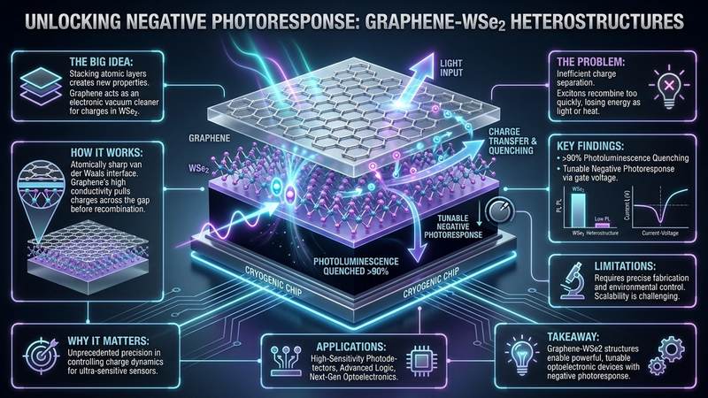
The Problem This Research Is Solving
In the quest to build better optoelectronic devices, such as photodetectors and solar cells, the primary challenge is managing how charges move at the interface between different materials. When light hits a semiconductor like WSe2, it creates an exciton, which is essentially a bound pair consisting of an electron and a hole. For this light to be converted into a usable electrical signal, these pairs must be split apart efficiently and the resulting charges must be swept away before they can recombine. If they recombine too quickly, the energy is lost as light (photoluminescence) or heat, rendering the device inefficient.
Furthermore, most conventional photodetectors exhibit a positive photoresponse, meaning that when light hits the material, the electrical current increases. While useful, having a device that can only respond in one direction limits the complexity of the logic circuits and the types of sensing mechanisms that can be implemented. Researchers have long sought a way to precisely modulate this response, specifically finding a mechanism to trigger a negative photoresponse—where light actually causes the current to drop—and doing so in a way that can be tuned externally. Understanding how to manipulate the tunneling barrier between layers is the key to unlocking this control, but achieving a stable, high-performance interface has remained an elusive goal.
This complex puzzle was addressed in a detailed study conducted by Yao Feng, Ze Cao, Longkun Yang, Mingyu Shi, Yujing Fan, Z P Huang, Mohamed Abid, Fengjiang An, Huei‐Ru Fuh, Yuh‐Renn Wu, Ching‐Ray Chang, and Han‐Chun Wu. Their work focuses on how the mere proximity of graphene to WSe2 fundamentally alters the way light and electricity interact within the material stack.
The Key Idea in Plain English
The central idea of this research is to use graphene as an electronic vacuum cleaner that siphons charges away from the WSe2 layer. Because graphene is incredibly conductive and has a specific electronic affinity, it creates a powerful pull on the charges generated within the WSe2 when light shines on it. By placing these two materials in a vertical stack, the researchers created a scenario where electrons and holes are forced to migrate across the interface.
The most striking part of this discovery is that by changing the electrical environment—specifically by using a gate voltage to alter the charge density—the researchers could change how the device reacts to light. They found that if they could make the barrier between the two materials thin enough, specifically under one nanometer, the physics of the device shifted. Instead of light increasing the current, it began to decrease it. This transition from a positive to a negative photoresponse is not a fluke but a controlled result of how charges accumulate at the interface and how they tunnel through the energy barrier separating the two layers.
How the Graphene-Based System Works
To understand how this system operates, one must first look at the nature of the van der Waals interface. Unlike traditional semiconductors that are grown together, which often results in lattice mismatches and defects that trap charges, these 2D layers are simply placed on top of one another. This preserves the intrinsic electronic properties of both graphene and WSe2.
When light is absorbed by the WSe2 layer, it excites an electron from the valence band to the conduction band, leaving behind a positive hole. In an isolated layer of WSe2, these electrons and holes would quickly find each other and recombine, emitting a photon of light in a process called photoluminescence. However, when graphene is placed on top, it creates a strong interfacial charge transfer. Because of the difference in their work functions, there is a natural drive for charges to move across the boundary. Specifically, graphene induces an effective hole depletion in the WSe2 layer. This means that the holes are pulled toward or pushed away from the interface in a way that prevents them from meeting the electrons.
This charge transfer is governed by the tunneling effect, a quantum mechanical phenomenon where a particle can pass through a potential energy barrier that it classically should not be able to cross. The width and height of this barrier determine how easily charges can move between the graphene and WSe2. By applying a gate voltage, the researchers can effectively change the height of this barrier or the amount of charge accumulated at the interface, thereby controlling the flow of electricity through the heterojunction.
What the Researchers Found
The findings of the study are highlighted by two major observations: ultrahigh photoluminescence quenching and a tunable photoresponse. The researchers discovered that when WSe2 is brought into proximity with graphene, the photoluminescence is quenched by more than 90 percent. This is a massive result. It proves that the charge transfer from WSe2 to graphene is so efficient and rapid that almost no excitons are left to recombine and emit light. Instead, the excitons are ripped apart almost instantly, with the charges being swept into the graphene layer.
Beyond this quenching effect, the team explored how the device responds to light under different electrical biases. They observed a transition from a positive photoresponse to a negative photoresponse. In the positive regime, light generates carriers that increase the conductivity of the device. However, as they reduced the effective tunneling barrier width to below approximately one nanometer, the behavior flipped.
In this negative photoresponse regime, the illumination of the device actually leads to a decrease in current. This happens because the light enhances the accumulation of charges at the interface, which in turn increases the effective tunneling barrier or modifies the local electric field in a way that hinders the flow of electrons. This creates a competitive dynamic between the bias-induced electric field, which tries to push charges through the device, and the interfacial charge transfer, which alters the barrier. The result is a device where light acts as a switch that can turn current down rather than up.
Why the Result Matters
This research is significant because it demonstrates a level of precision in controlling charge dynamics that is rarely seen in optoelectronic materials. The ability to achieve over 90 percent quenching indicates that graphene is an ideal partner for any semiconductor where the goal is to separate charges as quickly as possible. This has direct implications for the efficiency of light-harvesting devices, as it suggests that we can minimize energy loss through recombination.
Even more important is the discovery of the negative photoresponse transition. In the world of computing and signal processing, having a material that can provide both positive and negative responses to the same stimulus allows for the creation of more complex logic gates. For example, a sensor that can flip its polarity based on a gate voltage could be used to create highly sensitive differential detectors or optical switches that operate with extremely low power.
Moreover, the fact that this behavior is governed by a tunneling barrier of less than one nanometer gives engineers a concrete target for fabrication. It proves that the thickness of the interface is not just a structural detail but a primary lever for controlling the electrical signature of the device.
Limitations and What Still Needs Testing
While these results are groundbreaking, there are several hurdles before such a device enters commercial production. The current fabrication method relies on the vertical stacking of 2D flakes, a process that is often performed on a small scale in laboratory settings. To make this commercially viable, the industry would need to develop methods for large-area growth and transfer of these heterostructures without introducing contamination or wrinkles that could disrupt the one-nanometer precision required for the tunneling barrier.
Additionally, the stability of the van der Waals interface over long periods of operation needs further investigation. Because the layers are not chemically bonded, environmental factors such as humidity or temperature fluctuations could potentially shift the alignment of the layers or introduce interfacial impurities, which would alter the tunneling behavior and the photoresponse. More testing is required to determine how these devices perform under extreme conditions and whether the negative photoresponse remains consistent across thousands of cycles of illumination.
Real-World Applications
The practical applications for this graphene/WSe2 architecture are vast. One immediate application is in the field of ultra-sensitive photodetectors. Because the device can be tuned to a negative photoresponse, it could be used in specialized imaging systems that require high contrast or specific signal modulation to filter out background noise.
In the realm of energy, these findings could lead to more efficient organic and inorganic solar cells. By integrating graphene-like layers to quench photoluminescence and sweep away charges, designers can create cells that capture more of the sunlight's energy before it is lost to heat.
Furthermore, this research paves the way for new types of optical modulators in telecommunications. A device that can switch its current response based on light and gate voltage could act as a high-speed optical switch, directing data streams in photonic circuits with much higher efficiency than current silicon-based components.
If You Remember One Thing
If there is one key takeaway from this research, it is that the proximity of graphene to a semiconductor like WSe2 creates a powerful electronic synergy. By carefully controlling the interface at a scale of less than one nanometer, researchers can effectively flip how a material responds to light, moving from an increase in current to a decrease in current. This level of tunability transforms the material from a simple sensor into a sophisticated electronic switch.
FAQ
What is a van der Waals heterojunction?
It is a structure made by stacking two-dimensional materials on top of each other. Unlike traditional junctions, these layers are held together by weak van der Waals forces rather than strong chemical bonds, which allows the materials to maintain their unique properties without being distorted by a lattice mismatch.
What does it mean when photoluminescence is quenched?
Photoluminescence occurs when a material absorbs light and then re-emits it. Quenching is the process of stopping that emission. In this research, quenching happens because graphene pulls the electrons and holes away from each other so quickly that they cannot recombine to emit light.
Why is a negative photoresponse unusual?
Most light sensors are designed so that more light equals more electrical current. A negative photoresponse means that as the light intensity increases, the electrical current actually goes down. This is counterintuitive and allows for more complex ways of processing signals in electronic circuits.
How does the gate voltage affect the device?
The gate voltage acts like a remote control for the electrons in the system. By changing the voltage, researchers can adjust the density of charges at the interface and modify the height of the energy barrier that electrons must tunnel through, which in turn changes how the device responds to light.
Is this technology ready for use in consumer electronics?
Not yet. While the physics has been proven in a laboratory setting, scaling the production of these atomic-layer stacks to a commercial level requires more advanced manufacturing techniques to ensure every device has the exact same interface thickness and purity.
Conclusion
The study of graphene/WSe2 heterojunctions reveals the profound impact that atomic-scale proximity has on the behavior of light and electricity. By leveraging the exceptional conductivity of graphene and the light-absorbing properties of WSe2, Yao Feng and their colleagues have demonstrated that we can manipulate charge transfer with incredible precision. The discovery of ultrahigh photoluminescence quenching and the ability to trigger a negative photoresponse by narrowing a tunneling barrier to under one nanometer represents a significant leap forward. While challenges in mass production remain, the fundamental physics established here provide a blueprint for a new generation of tunable, high-efficiency optoelectronic devices that could one day redefine how we sense and process light.
Evaluate Our Quality
Serious about B2B integration? Test our premium Pulsed Electrical Resistive Carbon Heating turbostratic graphene in your lab. 100g sample packs available now.