Seeing the Invisible: Machine Learning and Resistance Tomography for Graphene Quality Control
Imagine a high-performance electronic component that looks flawless under the most powerful microscope available, yet fails to conduct electricity. For engineers building the next generation of flexible sensors and carbon-based electronics, this is a terrifying prospect. These are known as subvisual defects—failures that destroy the function of a material without leaving a visible scar or structural crater. Because graphene is often used in porous, three-dimensional architectures, a break in the internal conductive pathway can render a device useless while the surface remains visually pristine.
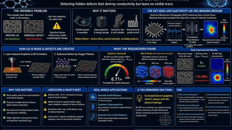
The Problem This Research Is Solving
The manufacturing of laser-induced graphene, or LIG, has opened new doors for rapid prototyping of electrodes and sensors. However, as these devices scale up in size and complexity, ensuring quality control becomes a massive hurdle. Traditional imaging techniques, such as optical microscopy and scanning electron microscopy, rely on morphological signatures. In other words, they look for physical changes like cracks, holes, or debris.
The critical issue is that electrical failure does not always correlate with physical deformation. A material can maintain its overall shape and structural integrity while losing the internal connectivity required for electrons to move efficiently. When these functional degradations occur without a change in morphology, they are labeled subvisual defects. If an engineer cannot see the defect and cannot locate it precisely, they cannot fix the manufacturing process or predict when a device will fail. This creates a bottleneck in the production of large-area carbon electronics, where a single microscopic break in a conductive network can compromise an entire system.
The Key Idea in Plain English
To solve this, K. Minakawa, Kotaro Takanashi, Yuki Kimura, Annop Klamchuen, Winadda Wongwiriyapan, and Takashi IKUNO developed a diagnostic approach called machine-learning-assisted electrical resistance tomography, or ML-ERT. Instead of using light or electrons to take a picture of the surface, they use electricity itself as the imaging medium.
Think of this like an ultrasound or a CT scan, but for electrical conductivity. By applying small currents to the edges of a graphene sample and measuring how those currents flow through the material, the system can create a map of the internal resistance. However, translating these raw electrical measurements back into a visual map of where the defect is located is mathematically difficult. This is known as the inverse problem. To overcome this, the researchers integrated a one-dimensional convolutional neural network, which is a type of artificial intelligence trained to recognize the specific electrical signatures associated with various defect locations. The AI acts as a translator, turning complex resistance data into a precise coordinate of the failure.
How the Graphene-Based System Works
Laser-induced graphene is created by using a high-energy laser to convert carbon-rich polymers, such as polyimide, into a porous network of graphene flakes. This structure is highly prized because its porosity provides a massive surface area, which is ideal for supercapacitors and chemical sensors. The conductivity of LIG depends on the continuous overlap and connection of these graphene flakes; as long as there is a connected path of sp2-hybridized carbon, electrons can zip through the material.
To test their detection system, the researchers needed to create defects that were truly invisible. They used masked oxygen plasma irradiation. In this process, an oxygen plasma is exposed to the graphene. The highly reactive oxygen atoms attack the carbon lattice, reacting with the graphene to form volatile carbon dioxide and carbon monoxide gas. This effectively etches away the carbon atoms, breaking the conductive bridges between graphene flakes.
Crucially, by controlling the intensity and duration of the plasma, the researchers could destroy the electrical connectivity without collapsing the physical skeleton of the porous graphene. This resulted in a dramatic increase in electrical resistance—up to four orders of magnitude higher than the original state—while the material remained indistinguishable under a microscope. The cause and effect here are clear: the oxygen plasma removes enough carbon to sever the electron pathways (the function), but not enough to alter the overall thickness or surface texture of the LIG (the morphology).
What the Researchers Found
The core of the discovery lies in the sensitivity and accuracy of the ML-ERT framework. The researchers found that the system could successfully pinpoint these hidden defects once the resistance contrast reached a specific threshold. Specifically, when the ratio of the defected resistance to the original resistance was 6.71 or higher, the machine learning model could accurately localize the failure.
To understand why this happened at a physical level, the team employed 3D finite element analysis. This is a computational method that simulates how electricity flows through complex geometries. The simulation revealed that the tomographic contrast—the ability of the system to see the defect—is driven by an effective conductive volume loss. When more than 30 percent of the internal conductive pathways in a specific region are destroyed, the electrical flow is diverted so significantly that it creates a detectable signature at the boundaries of the sample.
This means the ML-ERT system is not just guessing; it is measuring the actual loss of conductive volume. The convolutional neural network was able to learn the non-linear relationship between these volumetric losses and the resulting voltage drops measured at the edges, allowing it to map the internal state of the graphene with high precision.
Why the Result Matters
This research is a major step forward because it moves quality control from subjective visual inspection to objective functional mapping. In the world of carbon electronics, a device that looks perfect but does not work is a failure. By providing a way to visualize electrically critical failures that are optically invisible, this method allows manufacturers to identify exactly where their production process is failing.
For example, if a specific area of a large-area LIG sensor consistently shows subvisual defects under ML-ERT, engineers can trace that back to a fluctuation in laser power or a contamination issue during the synthesis process. Because the method is nondestructive, it can be used to test components before they are integrated into larger systems, ensuring that only functionally perfect materials move forward in the assembly line. This reduces waste and increases the reliability of graphene-based technology, making it more viable for industrial applications.
Limitations and What Still Needs Testing
While the results are promising, the system is not without limitations. The most significant constraint is the resistance threshold. If a defect is too mild—meaning it increases resistance by less than 6.71 times the original value—the ML-ERT system may struggle to localize it accurately. This suggests that very subtle degradations might still slip through the cracks of this diagnostic tool.
Furthermore, the current model relies on a convolutional neural network that must be trained on specific types of defects. It remains to be seen how the system would perform when faced with a variety of different defect types simultaneously, such as a mix of chemical contamination and physical cracks. Future testing will need to determine the limits of the system's resolution; while it can find a defect, there is a limit to how small that defect can be before its electrical signature becomes indistinguishable from the background noise of the material's inherent porosity.
Real-World Applications
The most immediate application for ML-ERT is in the quality assurance of large-area carbon electronics. This includes the production of flexible electrodes for wearable health monitors, where a break in the conductive path could lead to inaccurate heart rate or glucose readings.
Beyond simple electrodes, this technology could be applied to the development of graphene-based supercapacitors. In these devices, the efficiency depends on the connectivity of the porous network to the current collector. Using ML-ERT, manufacturers could map the uniformity of the conductive volume across a large capacitor sheet, ensuring that energy is stored and released evenly across the entire surface.
Additionally, this approach could be used in the field of electronic skins or soft robotics. These devices are often subjected to mechanical stress that can cause internal fatigue and subvisual fractures. ML-ERT could serve as a diagnostic health check, allowing engineers to detect internal degradation before the device suffers a total catastrophic failure.
If You Remember One Thing
The most important takeaway is that functional failure in graphene does not always look like physical damage. By combining electrical resistance tomography with machine learning, researchers can now detect and locate invisible defects that destroy conductivity but leave the structure intact, providing a vital new tool for ensuring the reliability of carbon-based electronics.
FAQ
What is laser-induced graphene?
Laser-induced graphene is a material created by using a laser to heat carbon-containing polymers, which transforms them into a porous, conductive network of graphene. It is popular because it is fast to make and has a high surface area, making it great for sensors.
What does subvisual defect mean?
A subvisual defect is a failure in the material's function—such as a loss of electrical conductivity—that does not cause any visible change in the material's appearance, even when viewed under a high-powered microscope.
How does electrical resistance tomography work?
It works by applying an electrical current to the edges of a sample and measuring the resulting voltage. By analyzing how the electricity flows through the material, the system can create a map of where the resistance is higher or lower.
Why was machine learning necessary for this research?
The relationship between the electrical measurements at the edge and the actual location of a defect inside the material is very complex. A convolutional neural network was used to solve this inverse problem, effectively learning how to translate raw data into a precise location map.
Is this method used in commercial products yet?
The research demonstrates a successful proof-of-concept for quality control. While it provides a definitive solution for detecting hidden failures, further testing on various defect types and scales is required before it becomes a standard industrial tool.
Conclusion
The ability to see the invisible is a recurring theme in scientific progress, from X-rays to infrared imaging. In the realm of carbon electronics, ML-ERT represents a similar leap forward. By shifting the focus from how a material looks to how it functions, K. Minakawa and their colleagues have provided a roadmap for the reliable production of graphene devices. As we move toward a future of flexible, wearable, and highly integrated electronics, the ability to non-destructively diagnose internal failures will be essential. This marriage of materials science, electrical engineering, and artificial intelligence ensures that the potential of graphene is not hindered by the invisible flaws of its own creation.
Evaluate Our Quality
Serious about B2B integration? Test our premium Pulsed Electrical Resistive Carbon Heating turbostratic graphene in your lab. 100g sample packs available now.