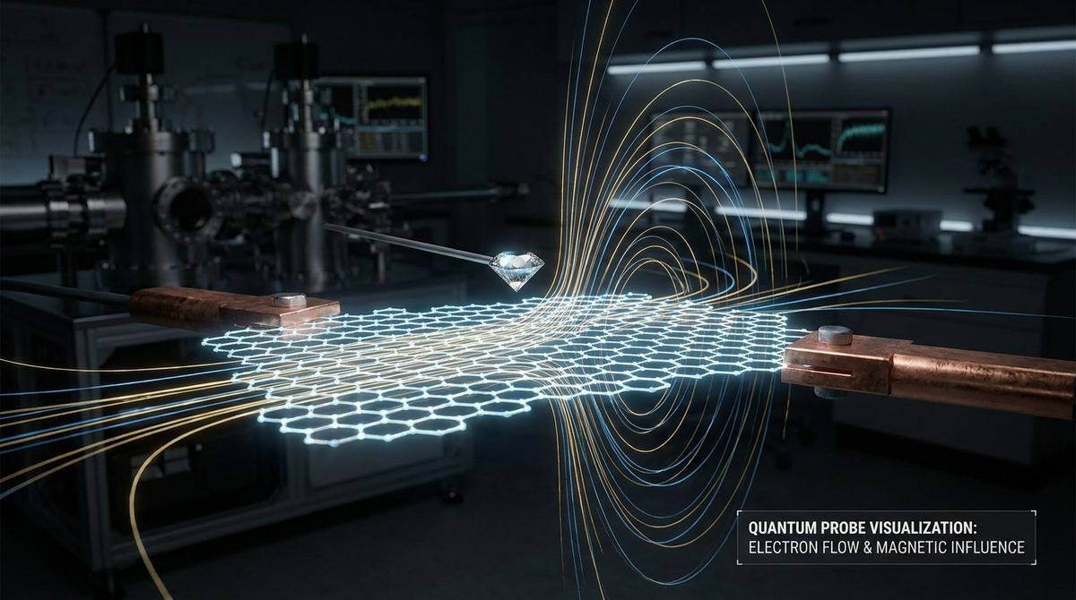
Imagine trying to understand why a city's traffic is congested by only looking at the total number of cars entering and leaving the city limits. You would know that there is a slowdown somewhere, but you would have no way of knowing which specific intersection is clogged or where drivers are taking detours to avoid a crash. For decades, this has been the fundamental limitation in condensed matter physics. Scientists studying electricity in materials like graphene have relied on bulk resistance measurements, which provide an average value for the entire device but hide the microscopic chaos happening inside. This research changes that by providing a high-resolution map of exactly where electrons go and why they divert, turning a blind measurement into a visual experience.
The Problem This Research Is Solving
The primary challenge in developing next-generation electronics with two-dimensional materials is the interface. When a three-dimensional metal lead is connected to a one-atom-thick sheet of graphene, the transition is not seamless. There is often a significant jump in electrical resistance at this boundary, known as contact resistance. This resistance occurs because of the mismatch in the density of electronic states between the bulk metal and the thin graphene layer, as well as potential chemical contamination or structural defects at the point of contact.
Until now, researchers could only infer the existence of these problems by measuring the total voltage drop across a device. They knew that if the resistance was high, the interface was poor, but they could not see if the current was flowing evenly across the contact or if it was crowding into a tiny fraction of the available area. This lack of spatial information makes it incredibly difficult to optimize device geometry or understand how external forces, such as magnetic fields, influence the flow of electrons at a local level. Without direct imaging, scientists were essentially guessing the internal architecture of current distribution based on a single output number.
The Key Idea in Plain English
To solve this, C. Ding, Marius L. Palm, Kevin Kohli, Takashi Taniguchi, Kenji Watanabe, and Christian L. Degen developed a way to use a quantum sensor as a microscopic magnifying glass for electricity. The core principle relies on the fact that any electrical current flowing through a conductor creates a tiny magnetic field around it. By using a single-spin quantum magnetometer—specifically a nitrogen-vacancy center in a diamond tip—the researchers could scan the surface of a graphene device and detect these minute magnetic fields.
By measuring the strength and direction of the magnetic field at every single point across the device, they could mathematically reconstruct the path of the current flowing beneath them. This is similar to how a geologist might use a magnetometer to find buried pipes or mineral deposits; however, this process happens at the nanoscale and with enough precision to see electrons reacting to external magnetic fields in real-time. This allowed the team to move beyond bulk resistance and actually watch the current bend and shift as it moved from the metal into the graphene.
How the Graphene-Based System Works
Graphene is an ideal candidate for this type of study because of its unique electronic structure. In most materials, electrons behave like particles with a specific mass, but in graphene, they behave like massless Dirac fermions. This occurs because the carbon atoms are arranged in a hexagonal honeycomb lattice, creating a linear energy-momentum relationship known as the Dirac cone. This structure allows electrons to move at incredibly high speeds with minimal scattering, which is why graphene has such high intrinsic conductivity.
In the system designed for this study, a thin layer of graphene was integrated with metal electrodes to create a hybrid device. The transport of electrons in this setup is governed by several competing factors. First, there is the intrinsic magnetoresistance of the graphene, which changes based on how the electrons move around the Dirac cone. Second, there is the phenomenon of carrier hydrodynamics, where electrons in ultra-pure graphene behave more like a viscous fluid than a gas of independent particles, flowing in streamlines rather than random paths. Finally, the interface between the metal and graphene acts as a bottleneck, where the chemistry of the bond and the physical geometry of the contact dictate how easily electrons can jump from the 3D electrode into the 2D sheet.
What the Researchers Found
The researchers discovered that when they applied an external magnetic field of approximately 0.5 Tesla, the current flow did not remain in a straight line. Instead, they directly observed the Lorentz deflection of the current. The Lorentz force is a fundamental physical law stating that a charged particle moving through a magnetic field experiences a force perpendicular to both its velocity and the field direction. In bulk measurements, this manifests as a change in resistance, but under the quantum sensor, it appeared as a visible bending of the current streamlines near the graphene-metal interface.
Specifically, they found that the current distribution was highly non-uniform. The flow tended to crowd toward the edges of the contacts, a phenomenon driven by the interplay between the device geometry and the local contact resistance. By combining these visual maps with global resistance data, the team revealed that the total transport properties were not just a result of the graphene itself, but were heavily governed by how the current was forced to divert at the interfaces. They were able to quantitatively map spatial variations in contact resistance across the interface, proving that some areas of the contact were significantly more efficient than others, even within a single junction.
Why the Result Matters
This result is significant because it provides a diagnostic tool for the atomic-scale engineering of electronic devices. For years, the industry has struggled with the fact that 2D materials often underperform in real-world devices compared to their theoretical potential. This research proves that the bottleneck is often not the material itself, but the interface where the material meets the rest of the circuit.
By being able to see exactly where current crowds or diverts, engineers can now redesign contact geometries to minimize resistance. Furthermore, the ability to visualize carrier hydrodynamics and Lorentz deflection at room temperature opens a new window into quantum transport. Understanding how electrons flow as a fluid rather than individual particles could lead to the development of electronics that generate far less heat, as hydrodynamic flow is more efficient and reduces the energy lost to scattering.
Limitations and What Still Needs Testing
While this achievement is a breakthrough in imaging, it is important to note that this method is currently a diagnostic tool rather than a manufacturing process. The scanning single-spin quantum sensor requires an extremely stable environment and takes a significant amount of time to map a single device point by point. It is not yet fast enough to be used for real-time monitoring during the fabrication of chips.
Additionally, while the researchers successfully imaged transport at 0.5 Tesla, further testing is needed to see how these patterns evolve at much higher magnetic fields or at cryogenic temperatures where quantum effects like the Quantum Hall Effect become dominant. There is also a need to test this technique on other 2D materials, such as transition metal dichalcogenides, to see if the interface resistance behaves similarly across different classes of two-dimensional semiconductors.
Real-World Applications
The most immediate application of this research is in the quality control and optimization of graphene-based sensors and transistors. By imaging the current flow, manufacturers can identify "dead zones" in their contacts and adjust their chemical deposition or etching processes to ensure a more uniform interface. This would directly lead to devices with lower power consumption and higher switching speeds.
Beyond simple electronics, this technique could be applied to the development of spintronic devices, where the spin of the electron is used instead of its charge to process information. Since the sensor used in this study is sensitive to spin, it is uniquely positioned to image spin-currents, which are even harder to detect than traditional electrical currents. This could accelerate the creation of ultra-fast, non-volatile memory storage that requires almost no power to maintain data.
If You Remember One Thing
The most critical takeaway from this research is the transition from blind measurement to direct visualization. By using a diamond-based quantum sensor to map magnetic fields, researchers can now see exactly how electrons bend and crowd at the interface between graphene and metal, revealing that the secret to better 2D electronics lies in mastering the contact point rather than just the material itself.
FAQ
What is a single-spin quantum sensor?
It is a probe that uses a nitrogen-vacancy center in a diamond crystal. This center acts like a tiny atomic compass that is incredibly sensitive to local magnetic fields, allowing researchers to detect the presence of electrical currents passing beneath it.
What is the Lorentz deflection mentioned in the study?
This occurs when an electron moving through a magnetic field is pushed sideways. In this research, it caused the current flow in the graphene to bend, which was captured as a visual shift in the current map.
Why does contact resistance happen in graphene?
It happens because graphene is only one atom thick, while metal leads are bulk materials. This creates a mismatch in how many electrons can fit into a given energy level at the junction, creating a bottleneck that slows down the flow of electricity.
What are Dirac fermions?
These are electrons in graphene that behave as if they have no mass. This allows them to travel much faster and more efficiently than electrons in standard silicon, which is why graphene has such high conductivity.
Is this technology ready for use in home computers?
No, it is currently a laboratory imaging technique used for research and development. It helps scientists design better components, but the sensor itself is not a part of the final electronic device.
Conclusion
The work by C. Ding and colleagues represents a shift in how we approach condensed matter physics. By bridging the gap between global resistance measurements and local current imaging, they have provided a roadmap for overcoming the interface challenges that have long plagued 2D materials. The ability to visualize the Lorentz deflection and map contact resistance at the nanoscale ensures that future graphene devices will be designed based on visual evidence rather than theoretical approximations. As these quantum sensing techniques evolve, they will likely become standard tools in the quest to build faster, cooler, and more efficient quantum electronics.