
Revolutionizing Semiconductor Fabrication with Contactless Graphene Seeding
Explore a proposed shift from traditional Czochralski ingot growth to a contactless, graphene-seeded method that could reduce silicon waste by up to 70 percent.
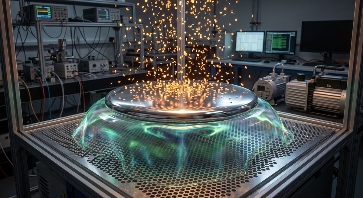
Almost every piece of modern technology, from the smartphone in your pocket to the servers powering the global internet, relies on thin slices of ultra-pure silicon known as wafers. For decades, the world has produced these wafers using a method that is surprisingly wasteful. To get those thin disks, engineers first grow a massive, heavy cylinder of silicon called an ingot and then use industrial diamond saws to slice it into wafers. This process creates a massive amount of wasted material, essentially turning high-purity silicon into dust during the cutting phase. It is a bit like carving a statue out of a giant block of marble only to find that half the stone ends up as shavings on the floor.
The current industry standard for producing silicon is the Czochralski process. In this method, molten silicon is held in a high-purity quartz crucible, and a single seed crystal is dipped into the melt and slowly pulled upward while rotating. This creates a large cylindrical ingot. However, this approach introduces two primary inefficiencies. First, there is the issue of contamination. The molten silicon is in direct contact with the quartz crucible, which can leach oxygen and other impurities into the silicon, potentially affecting the electrical properties of the final semiconductor.
Second, the geometric mismatch between a cylinder and a disk leads to what engineers call kerf loss. When a wire saw slices through a solid ingot to create wafers, a significant portion of the material is physically removed as sawdust. This waste is not just an environmental concern but a financial one, as high-purity silicon feedstock is expensive to refine. Kristopher Knudsen identifies these bottlenecks as fundamental flaws in the architecture of wafer fabrication and proposes a shift from a subtractive process—where we cut away waste—to a formative process, where the silicon is grown directly into its final flat shape.
The proposed solution moves away from the idea of growing a giant rod and instead focuses on creating a floating pancake of liquid silicon. Imagine a high-tech air hockey table where the puck is not plastic, but a pool of molten silicon. By blowing high-pressure argon gas upward through a perforated bed, the researchers propose to suspend the liquid silicon in mid-air. Because there is no container, there is no crucible to contaminate the melt.
Once the silicon is floating and shaped into a flat disk by gravity, it needs to be solidified. In traditional growth, this happens at a single point where the seed crystal meets the melt. The new idea uses graphene nanoparticles as distributed seeds. Instead of one seed crystal pulling a rod upward, thousands of tiny graphene flakes are carried by the argon gas and land across the entire surface of the liquid silicon simultaneously. This triggers the crystallization process across the whole disk at once, allowing the silicon to solidify directly into a flat wafer geometry without ever needing a saw.
The technical execution of this system relies on the intersection of fluid dynamics and materials science. The foundation is a quartz sieve bed featuring a variable-density pinhole array. By controlling the pressure of the argon gas flowing through these holes, the system creates a uniform gas cushion. This cushion acts as a physical barrier that supports the weight of the molten silicon via pressure equilibrium. Because the liquid does not touch any solid surface during this phase, the risk of impurity diffusion from a crucible is virtually eliminated.
The most critical component, however, is the use of graphene for distributed seeding. In crystallography, nucleation is the process where atoms begin to arrange themselves into a structured lattice. This usually requires a seed or a surface to lower the energy barrier required for the first few atoms to lock into place. Graphene, a single layer of carbon atoms arranged in a hexagonal honeycomb lattice, serves as an ideal substrate for this purpose.
When graphene nanoparticles are suspended in the argon carrier gas and deposited onto the molten silicon, they provide a vast number of nucleation sites across the entire surface area of the melt. The high thermal conductivity of graphene helps manage the local temperature at these interface points, while its structural stability allows it to act as a template for the silicon atoms. As the system cools, the silicon atoms align with these distributed seeds, causing the rest of the liquid to crystallize in a planar fashion rather than a linear one. This effectively transforms the growth process from a vertical pull into a surface-wide solidification event.
The primary finding of this architectural proposal is a theoretical and structural shift in how we perceive semiconductor waste. By eliminating the need for cylindrical ingot growth and subsequent slicing, the researchers estimate that silicon feedstock waste could be reduced by 50 to 70 percent. This is a staggering figure when considering the global scale of chip production.
Furthermore, the research indicates that this method removes the dependency on high-purity quartz crucibles, which are not only expensive but also subject to thermal stress and degradation over time. By utilizing an argon pressure cushion, the system replaces a consumable chemical container with a reusable mechanical gas delivery system. The result is a process that produces a flat geometry by default, potentially removing the need for the kerf-heavy slicing steps that define the current industrial landscape.
The implications of this research extend beyond simple cost savings. In the semiconductor industry, purity is everything. Even a few parts per billion of an unwanted element can change how a transistor switches or how an electron moves through a channel. By removing the crucible from the equation, this contactless method could lead to silicon wafers with significantly lower levels of oxygen contamination, potentially enhancing the performance and reliability of high-end microprocessors.
From an environmental perspective, reducing feedstock waste by over half would drastically lower the energy requirements for refining metallurgical-grade silicon into electronic-grade silicon. The refining process is incredibly energy-intensive, requiring temperatures upwards of 1,100 degrees Celsius. If we can produce more wafers from the same amount of raw material, the overall carbon footprint of every chip in every device on earth would decrease.
While the theory is sound, it is important to note that this architecture is a proposal for a new fabrication method rather than a commercially deployed technology. Several significant engineering hurdles remain. The first is the stability of the argon cushion. Maintaining a perfectly uniform pressure across a large surface area while supporting the weight of molten silicon is a complex fluid dynamics problem. Any fluctuation in gas pressure could lead to ripples or instabilities in the liquid, resulting in wafers that are not perfectly flat.
Additionally, the distribution of graphene nanoparticles must be precisely controlled. If the seeds are not distributed uniformly, some areas of the wafer might crystallize faster than others, leading to internal stresses and structural defects known as dislocations. These defects can ruin the electrical properties of the silicon. Finally, the thermal gradient across a wide, flat surface is very different from that of a narrow cylinder. Ensuring that the entire disk cools at a uniform rate to prevent cracking or warping will require sophisticated thermal management systems that have yet to be fully mapped out.
If successfully scaled, this technology would first find a home in the production of high-performance computing chips and AI accelerators, where purity and material efficiency are paramount. It could also revolutionize the solar energy sector. Solar cells use large quantities of silicon, and reducing the cost of wafer production by 50 to 70 percent could significantly lower the price of photovoltaic panels, accelerating the global transition to renewable energy.
Moreover, this contactless growth method could be adapted for other semiconductor materials beyond silicon. Gallium nitride or silicon carbide, which are used in power electronics for electric vehicles, often face challenges with substrate quality and waste. A gas-cushion approach combined with specialized 2D material seeding could provide a blueprint for the next generation of wide-bandgap semiconductors.
The core breakthrough here is the transition from subtractive manufacturing to formative growth. By using an argon gas cushion to float molten silicon and graphene nanoparticles to seed it across its entire surface, we can grow flat wafers directly, eliminating the wasteful process of slicing cylinders into disks.
What exactly is kerf loss in silicon production?
Kerf loss refers to the material that is turned into dust when a diamond saw slices through a silicon ingot. Because the saw blade has a certain thickness, it physically removes a thin layer of silicon with every cut, which cannot be easily recovered and results in significant waste.
Why is graphene used instead of other materials for seeding?
Graphene provides an excellent atomic template for silicon to grow upon because of its structure and high thermal conductivity. It lowers the energy required for nucleation, allowing the liquid silicon to solidify more efficiently across a wide surface area rather than at a single point.
How does a gas cushion prevent contamination?
In traditional growth, molten silicon sits in a quartz crucible, which can dissolve slightly into the melt. By floating the silicon on a cushion of argon, a noble gas that does not react with other elements, the silicon never touches a solid container, removing the source of crucible-based impurities.
Is this technology currently being used to make computer chips?
No, this is currently a proposed architecture and theoretical model. It provides a roadmap for how wafers could be grown in the future, but it still requires rigorous experimental testing to ensure stability and purity at an industrial scale.
Would this process make electronics cheaper for consumers?
Potentially. By reducing the waste of expensive high-purity silicon by 50 to 70 percent and removing several steps from the manufacturing chain, the overall cost of producing wafers could drop, which may eventually lower the cost of the chips used in consumer electronics.
The proposal for contactless flat wafer growth represents a bold reimagining of one of the most fundamental processes in modern industry. By combining the physics of gas cushions with the unique properties of graphene, this method addresses the dual challenges of material waste and chemical contamination. While the path from theoretical architecture to factory implementation is long and fraught with engineering challenges, the potential reward—a sustainable, high-purity, and efficient way to create the building blocks of the digital age—is too significant to ignore. Moving away from the Czochralski method could mark the beginning of a new era in materials science where we no longer carve our technology out of stone, but grow it with precision.
Serious about B2B integration? Test our premium Pulsed Electrical Resistive Carbon Heating turbostratic graphene in your lab. 100g sample packs available now.
Explore More
Explore a proposed shift from traditional Czochralski ingot growth to a contactless, graphene-seeded method that could reduce silicon waste by up to 70 percent.

This technical exploration examines how varying the length of chitosan chains on graphene sheets affects the loading and stability of the anticonvulsant Primidone, identifying a dimer configuration as the optimal carrier for improved bioavailability.

Researchers have developed a high-performance supercapacitor electrode by fusing liquid gallium and indium with reduced graphene oxide into a lightweight aerogel, combining fast charging with high energy density.