Revolutionizing Semiconductor Fabrication with Contactless Graphene Seeding
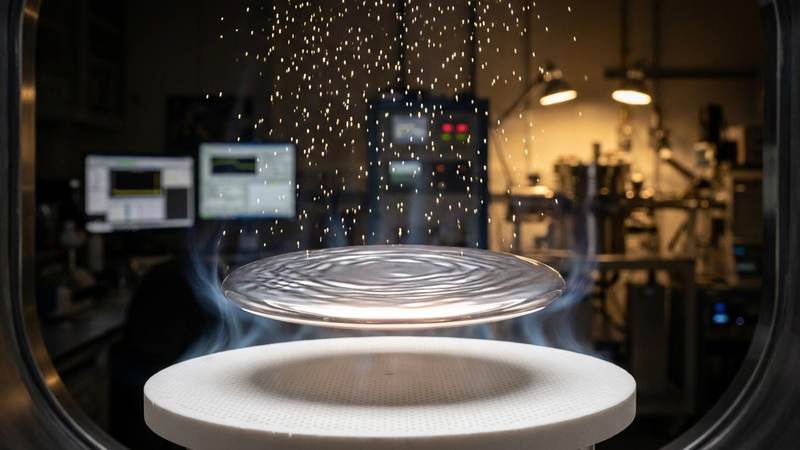
Imagine if the process of making computer chips was like carving a marble statue where you had to throw away half the block of marble as dust just to get the final shape. For decades, the semiconductor industry has operated exactly this way. To create the flat silicon wafers that power everything from smartphones to artificial intelligence, engineers grow massive cylindrical ingots and then slice them into thin discs using diamond saws. This slicing process creates a huge amount of waste known as kerf loss, where high-purity silicon is literally turned into powder and discarded. It is an inefficient legacy of the industrial age that has remained largely unchanged because the alternative was simply too difficult to engineer.
The Problem This Research Is Solving
The standard method for producing monocrystalline silicon is the Czochralski process. In this traditional setup, silicon is melted in a high-purity quartz crucible and a single seed crystal is dipped into the melt and slowly pulled upward to grow a large, cylindrical ingot. While effective, this method introduces two significant problems that Kristopher Knudsen seeks to address through a radical architectural redesign of wafer growth.
The first problem is contamination. Because the molten silicon sits in a quartz crucible at extreme temperatures, some of the oxygen from the quartz dissolves into the silicon melt. This unintentional doping can create defects in the crystal lattice or alter the electrical properties of the final chip, forcing manufacturers to spend immense energy and money purifying the material or managing these impurities through complex chemical processes.
The second problem is geometric waste. A cylinder is not a disc. When a manufacturer slices a cylindrical ingot into wafers, the saw removes a significant portion of the material as sawdust. This kerf loss represents a massive inefficiency in feedstock usage. Furthermore, the energy required to grow a giant ingot only to slice most of it away is an environmental and financial burden. The industry has long dreamed of growing silicon directly into its final flat wafer geometry, but the physics of surface tension and contamination made this nearly impossible until now.
The Key Idea in Plain English
The core innovation proposed here is to stop treating silicon like a solid beam that needs to be cut and start treating it like a liquid that can be shaped by air. Instead of using a crucible as a container, the system uses a cushion of high-pressure argon gas to float the molten silicon. Think of this like an air hockey table, but instead of a puck, you have a pool of white-hot liquid metal.
By pushing argon gas upward through a specialized sieve, the researchers create a pressure barrier that prevents the molten silicon from ever touching a solid surface. Because the silicon is floating and not constrained by the walls of a crucible, gravity naturally pulls it into a flat, disc-like shape. To turn this liquid pool into a solid crystal, the system introduces graphene nanoparticles via the gas stream. These particles act as tiny seeds that tell the silicon how to crystallize across the entire surface at once, rather than growing from a single point upward.
How the Graphene-Based System Works
The technical execution of this process relies on the precise interaction between fluid dynamics and materials science. The foundation is a flat quartz sieve bed featuring a variable-density pinhole array. This array is critical because it ensures that the argon gas is delivered with uniform pressure across the entire surface area. If the pressure were uneven, the molten silicon would tilt or ripple, ruining the flatness of the final wafer. By modulating the density of these pinholes, the system creates a stable gas cushion that supports the weight of the melt without allowing any liquid to leak through.
Once the molten silicon is floating and shaped by gravity, the focus shifts to crystallization. In traditional growth, a single seed crystal dictates the orientation of the entire ingot. This process is slow because the crystal must grow atom by atom from the bottom up. The proposed system replaces this with distributed graphene seeding. Graphene nanoparticles are suspended in the argon carrier gas and delivered directly onto the surface of the melt.
The role of graphene here is not just as a filler, but as a structural template. Graphene consists of a single layer of carbon atoms arranged in a hexagonal lattice. This structure provides an incredibly high surface-area-to-volume ratio and a specific electronic interface that lowers the energy barrier for silicon nucleation. When these nanoparticles hit the molten silicon, they act as thousands of simultaneous nucleation points. Because graphene is chemically stable at high temperatures and possesses a crystalline structure that can influence the alignment of surrounding atoms, it encourages the silicon to solidify into a consistent crystalline form across the entire flat surface simultaneously. This transforms the growth process from a linear climb into a parallel solidification event.
What the Researchers Found
The theoretical framework suggests that this contactless approach fundamentally changes the economics and purity of wafer production. By eliminating the quartz crucible entirely, the system removes the primary source of oxygen contamination. The absence of a solid container means there is no chemical reaction between the molten silicon and a vessel wall, resulting in a higher intrinsic purity of the silicon crystal.
More importantly, the researchers estimate that this architecture could reduce silicon feedstock waste by 50 to 70 percent. This staggering number comes from the elimination of the Czochralski ingot phase. Since the silicon is grown directly into a flat wafer geometry, the need for wire saw slicing vanishes. The kerf loss—the silicon dust created during slicing—is effectively eliminated because there is no sawing involved. Instead of wasting material to achieve a shape, the system uses physics and gas pressure to create the shape from the start.
Why the Result Matters
The implications of this research extend beyond simple waste reduction. In the semiconductor world, purity is everything. The ability to grow silicon without crucible contamination allows for the creation of devices with tighter tolerances and better electrical performance. When oxygen impurities are reduced, the mobility of electrons within the silicon can be more precisely controlled, which is essential as we push toward smaller transistors and faster processing speeds.
From a sustainability perspective, the reduction in feedstock waste is transformative. Producing high-purity polysilicon is an energy-intensive process involving hazardous chemicals and massive amounts of electricity. Reducing the amount of raw material needed by over half would significantly lower the carbon footprint of every chip produced. Furthermore, removing the dependency on high-purity quartz crucibles simplifies the supply chain, as manufacturers would no longer need to source specialized containers that can withstand extreme heat without melting or contaminating the melt.
Limitations and What Still Needs Testing
While the proposed architecture is revolutionary, it remains a conceptual design that faces significant engineering hurdles before it can enter a factory. One of the primary concerns is the stability of the argon cushion over larger diameters. While a small disc might float easily, maintaining a perfectly flat surface for a 300mm wafer requires extreme precision in gas flow. Any turbulence in the argon stream could introduce ripples or waves into the molten silicon, leading to thickness variations that would render the wafer useless.
There is also the question of graphene dispersion. For the distributed seeding to work, the graphene nanoparticles must be spread perfectly evenly across the surface. If the particles clump together or are delivered in uneven bursts, the silicon will crystallize at different rates, creating internal stresses and dislocations within the crystal lattice. These defects would act as traps for electrons, destroying the electrical conductivity required for semiconductors.
Finally, the thermal management of a floating melt is complex. In a crucible, heat is managed through the walls and the heating elements surrounding the vessel. In a contactless system, the researchers must develop a way to cool the molten silicon uniformly from the top and bottom to ensure a slow, controlled solidification process that avoids cracking due to thermal shock.
Real-World Applications
The most immediate application for this technology would be in the production of high-efficiency solar cells. Solar wafers do not always require the extreme purity levels of microprocessor wafers, meaning this contactless growth method could be implemented more quickly in the photovoltaic industry. Reducing the cost of silicon feedstock by 50 percent would dramatically lower the price of solar panels, accelerating the global transition to renewable energy.
Beyond solar, the technology could be used for specialized sensors and power electronics. Devices that operate at high voltages often require specific crystal orientations and ultra-high purity to prevent electrical breakdown. A contactless growth method that eliminates crucible impurities would provide a superior substrate for these high-power applications. If the system can be scaled, it will eventually target the logic chip market, potentially redefining how every CPU and GPU is manufactured.
If You Remember One Thing
If you remember one thing from this research, it is that we are moving toward a future where computer chips are grown like liquid mirrors rather than carved from stone. By using an argon gas cushion to float molten silicon and graphene nanoparticles to seed the crystal growth, we can eliminate the wasteful process of slicing ingots and remove the impurities caused by traditional crucibles.
FAQ
What is kerf loss in silicon manufacturing?
Kerf loss refers to the material that is turned into dust when a diamond saw slices through a cylindrical silicon ingot to create thin wafers. Because this powder cannot be easily reused in high-end chip making, it represents a massive waste of expensive, high-purity raw material.
How does argon gas help in this process?
Argon is an inert gas, meaning it does not react chemically with the molten silicon. By pumping it upward through a sieve, it creates a physical pressure cushion that supports the weight of the liquid silicon, allowing it to float without touching any solid surface.
Why is graphene used instead of other materials?
Graphene is chosen because its hexagonal carbon lattice provides an ideal template for silicon atoms to latch onto and organize. Its high surface area allows thousands of nanoparticles to act as simultaneous seeds, enabling the entire wafer to crystallize at once rather than growing from a single point.
Does this mean chips will become cheaper immediately?
No, because this is currently a proposed architecture rather than a commercially available product. Significant engineering is still required to ensure the gas cushion remains stable and the graphene is distributed evenly over large areas before it can be used in mass production.
Is the silicon produced this way different from normal silicon?
Potentially yes. Because the process eliminates the quartz crucible, there is less oxygen contamination. This leads to a higher purity crystal, which could result in chips that are faster, more efficient, and have fewer inherent defects.
Conclusion
The transition from Czochralski growth to contactless floating growth represents a paradigm shift in materials science. By leveraging the unique properties of graphene and the physics of gas pressure, this proposed method addresses the two greatest inefficiencies of the semiconductor industry: material waste and chemical contamination. While the path to industrial implementation requires solving complex challenges in fluid dynamics and thermal control, the potential rewards are too great to ignore. A world where silicon wafers are grown with minimal waste and maximum purity is a world where the ceiling for computing power and energy efficiency is pushed significantly higher.
Evaluate Our Quality
Serious about B2B integration? Test our premium Pulsed Electrical Resistive Carbon Heating turbostratic graphene in your lab. 100g sample packs available now.