Continuous Inert-Environment Manufacturing Framework for Boron/Graphene-Derived Conductive Nanothread Architectures: A Technical Deep Dive
Research conducted by: Joshua Nathaniel Friend
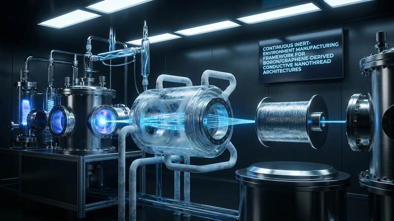
The groundbreaking conceptual manufacturing framework developed by Joshua Nathaniel Friend represents a pivotal leap forward in the scalable production of advanced conductive nanomaterials. By systematically addressing the inherent instabilities of boron and graphene hybrids during synthesis, this research establishes a viable pathway from laboratory-scale curiosities to industrial-scale continuous manufacturing. The integration of continuous spooling within a strictly controlled inert environment solves one of the most persistent bottlenecks in nanomaterial fabrication, paving the way for next-generation semiconductor architectures, high-capacity energy storage systems, and ultra-lightweight conductive composites. This technical report meticulously dissects the proposed architecture, exploring the vacuum-assisted manufacturing concepts, plasma-assisted deposition techniques, and cryogenic stabilization methodologies that make this continuous production framework a reality.
The Imperative of Strict Environmental Control and Oxidation Mitigation
The synthesis of boron-derived graphene nanothreads presents unique chemical and thermodynamic challenges, primarily due to the extreme reactivity of nascent nanoscale boron and carbon lattices when exposed to atmospheric conditions. Boron, in its highly reactive atomic state during deposition, possesses a profound affinity for oxygen and ambient moisture. Even trace amounts of atmospheric exposure can lead to the instantaneous formation of insulating boron oxide layers, which critically degrade the electron mobility and overall electrical conductivity of the final nanothread architecture. Consequently, the cornerstone of this manufacturing framework is the implementation of a rigorous, continuous inert-environment system.
The proposed architecture utilizes a cascading vacuum chamber design, employing a combination of roughing pumps, turbomolecular pumps, and advanced cryogenic pumps to achieve an ultra-high vacuum baseline. Once the baseline vacuum is established, the system is backfilled with ultra-high-purity inert gases, typically argon or nitrogen, which have been passed through specialized getter purifiers to reduce oxygen and moisture content to parts-per-billion levels. This dynamic inert atmosphere is continuously monitored by residual gas analyzers and mass spectrometers, ensuring that the environmental integrity remains uncompromised throughout the entire manufacturing cycle.
Furthermore, oxidation mitigation strategies extend beyond mere gas purity. The framework incorporates advanced flow dynamics to create localized laminar gas shields around the most critical synthesis zones. These laminar flows act as a secondary, kinetic barrier against any microscopic back-streaming of contaminants from downstream post-processing modules. By engineering the fluid dynamics of the inert gas, the system ensures that the delicate boron-graphene hybridization process occurs in a state of absolute chemical isolation, thereby preserving the intrinsic metallic or semiconducting properties of the nanothreads.
Plasma-Assisted Deposition Dynamics
At the heart of the continuous manufacturing framework lies the plasma-assisted deposition module. Traditional chemical vapor deposition techniques often require exceptionally high thermal budgets to crack precursor gases and initiate the nucleation of carbon and boron atoms. These extreme temperatures can lead to bulk agglomeration and the loss of the desired one-dimensional nanothread morphology. To circumvent this, the framework employs advanced plasma-enhanced chemical vapor deposition methodologies, utilizing high-frequency radio or microwave energy to excite the precursor gases into a highly reactive plasma state.
By ionizing precursor gases such as methane for the graphene backbone and diborane or boron trichloride for the boron integration, the system effectively lowers the activation energy required for atomic assembly. The plasma environment generates a rich mixture of radicals, ions, and excited neutral species that exhibit enhanced surface mobility when they interact with the catalytic growth substrate. This allows for the epitaxial growth of the boron-graphene lattice at significantly lower bulk temperatures, preserving the structural integrity of the continuous thread.
The precise tuning of the plasma parameters, including electron temperature, ion density, and residence time, is critical for controlling the stoichiometry of the boron doping within the graphene matrix. The framework proposes real-time optical emission spectroscopy to monitor the plasma chemistry, providing a feedback loop that dynamically adjusts the precursor gas flow rates and plasma power. This level of control ensures a uniform distribution of boron atoms within the sp-squared carbon lattice, which is essential for achieving the desired p-type semiconducting behavior or enhanced metallic conductivity characteristic of these advanced nanothread architectures.
Directional Nanothread Formation Mechanics
While plasma-assisted deposition provides the chemical building blocks, the physical architecture of the nanothreads dictates their ultimate utility in conductive applications. The framework introduces sophisticated directional formation mechanics to coax the depositing atoms into highly aligned, one-dimensional structures rather than amorphous thin films. This is achieved through the strategic application of external electromagnetic fields and highly controlled sheer forces within the deposition zone.
As the ionized species from the plasma approach the growth zone, a strong, static electric field is applied parallel to the desired axis of thread growth. Because the plasma species carry an electrical charge, they are subjected to electrostatic forces that guide their trajectory and influence their binding orientation upon the growing lattice. This field-directed assembly encourages the formation of long, continuous chains of boron-doped graphene, minimizing lateral branching and ensuring a high degree of structural anisotropy.
In addition to electrostatic guidance, the framework utilizes the physical dynamics of continuous extraction to promote alignment. As the nascent nanothread is continuously drawn from the reaction zone, it experiences a micro-scale mechanical tension. This applied stress effectively stretches the lattice during its most malleable formation phase, aligning the crystalline domains along the axis of tension. The synergy between the applied electromagnetic fields and the mechanical drawing forces results in a highly ordered nanothread with exceptional tensile strength and uninterrupted pathways for ballistic electron transport.
Cryogenic Stabilization and Thermal Gradient Engineering
Once the continuous nanothread emerges from the high-energy plasma deposition zone, it exists in a highly energetic and structurally vulnerable state. If allowed to cool at an uncontrolled rate, the kinetic energy of the atoms could lead to the formation of thermodynamic defects, such as Stone-Wales defects or amorphous carbon agglomerations, which act as scattering centers for electrons and severely degrade conductivity. To prevent this, the framework introduces a radical cryogenic stabilization phase immediately downstream of the deposition module.
The newly formed nanothread passes through a localized cryogenic zone, cooled by liquid nitrogen or liquid helium jackets, which rapidly quenches the material. This extreme and instantaneous drop in temperature effectively halts all atomic mobility, freezing the highly ordered crystalline structure established during the directional formation phase. This kinetic trapping preserves the ideal boron-graphene stoichiometry and prevents the phase segregation of boron atoms, which could otherwise occur if the material were allowed to reach thermodynamic equilibrium slowly.
Following this rigorous cryogenic stabilization, the nanothread enters a highly controlled thermal conditioning chamber. This phase involves thermal gradient engineering, where the thread is subjected to a precisely calibrated temperature profile. A gentle, incremental annealing process is applied in a pure argon environment to relieve any residual mechanical stresses introduced during the rapid quenching and continuous drawing phases. This careful thermal management heals minor lattice dislocations without imparting enough energy to disrupt the bulk structural integrity, ultimately optimizing the electrical conductivity and mechanical resilience of the final product.
Continuous Spool Extraction Methodologies
The transition from a static, batch-based synthesis process to a continuous manufacturing paradigm hinges on the successful implementation of the continuous spool extraction module. Handling nanoscale materials that are mere atoms thick requires extraordinary mechanical precision, as traditional spooling mechanisms would introduce catastrophic shear forces and immediately fracture the nanothreads. The framework outlines a specialized extraction architecture designed to operate seamlessly within the ultra-high vacuum environment.
The extraction system utilizes ultra-low-friction magnetic levitation bearings for all rotating components within the vacuum chamber. This eliminates the need for liquid lubricants, which would inevitably outgas and contaminate the inert environment. The tension applied to the nanothread during the winding process is controlled at the micro-Newton level using highly sensitive, non-contact optical tension sensors. These sensors utilize laser diffraction patterns to monitor the thread's tautness and diameter in real-time, feeding data back to the spooling motors to make instantaneous micro-adjustments to the rotational speed.
Furthermore, the spooling interface itself must be carefully engineered to prevent adhesion and structural damage to the nanothreads. The framework suggests the use of specialized, chemically inert polymer coatings on the collection spools, which provide a soft, non-abrasive landing surface for the nanomaterial. The entire spooling mechanism is housed within a modular airlock system, allowing fully loaded spools to be extracted and replaced with empty ones without breaking the main vacuum of the deposition and stabilization chambers, thereby ensuring truly continuous, uninterrupted manufacturing.
Modular Post-Processing and Semiconductor Integration
The ultimate value of these boron-derived graphene nanothreads lies in their integration into downstream applications, particularly within the semiconductor and advanced electronics industries. Recognizing this, the framework is designed with a highly modular post-processing architecture. Once the thread is stabilized and ready for collection, it can optionally be routed through a series of specialized, inline functionalization modules before final spooling.
For semiconductor applications, the nanothreads may require precise dielectric coatings to prevent short-circuiting when densely packed into microchip architectures. The framework allows for the integration of an inline atomic layer deposition module, which can uniformly coat the continuous thread with a nanometer-thick layer of insulating material, such as aluminum oxide or hafnium oxide, while still maintaining the inert vacuum environment. This immediate, in situ coating process is vastly superior to ex situ coating, as it guarantees that the pristine surface of the nanothread is never exposed to potential contaminants.
Additionally, the modular design accommodates inline slicing and matrix embedding technologies. For composite material manufacturing, the continuous thread can be fed directly into a polymer extrusion process, creating ultra-strong, lightweight, and conductive composite filaments suitable for advanced aerospace or automotive applications. By providing a scalable, customizable, and environmentally secure pathway from atomic synthesis to macro-scale integration, this manufacturing framework bridges the critical gap between theoretical nanomaterial science and practical, industrial-scale deployment.
Frequently Asked Questions
Question: What makes boron-derived graphene nanothreads superior to traditional copper conductors in electronic applications?
Answer: Boron-derived graphene nanothreads offer a unique combination of extreme tensile strength, low weight, and exceptional electrical properties. Unlike traditional copper, which suffers from electromigration and increased resistance at nanoscale dimensions, graphene-based structures can support ballistic electron transport, meaning electrons move with virtually no scattering. The addition of boron introduces specific p-type semiconducting characteristics or enhanced metallic states, making these nanothreads highly tunable for advanced microprocessors and flexible electronics where copper is reaching its physical scaling limits.
Question: Why is an inert environment absolutely necessary for this specific manufacturing process?
Answer: Both atomic carbon and boron are highly reactive when exposed to atmospheric conditions, particularly at the elevated temperatures required for synthesis. Boron has a very strong affinity for oxygen, and any exposure will rapidly form boron oxide insulators on the surface of the nanothreads, completely destroying their conductive properties. An inert environment, utilizing ultra-high vacuum and purified noble gases like argon, ensures that no oxygen, moisture, or atmospheric contaminants can interact with the delicate lattice during its formation, stabilization, and spooling phases.
Question: How does the cryogenic stabilization phase prevent structural degradation of the nanothreads?
Answer: After the nanothread is formed in the high-energy plasma zone, the atoms possess high kinetic energy. If cooled slowly, the atoms might rearrange into more thermodynamically stable but less conductive amorphous structures, or the boron might segregate from the carbon lattice. Cryogenic stabilization involves rapidly quenching the material with extreme cold, which instantly halts atomic movement. This kinetic trapping essentially freezes the atoms in their highly ordered, desired crystalline alignment, preserving the specific structural and electrical properties engineered during the deposition phase.
Question: What are the primary mechanical challenges in the continuous spool extraction of nanomaterials?
Answer: The primary challenge is applying the correct amount of mechanical tension to wind the material without fracturing it. Nanothreads, while possessing high tensile strength relative to their size, are incredibly fragile to macroscopic shear forces. The manufacturing framework addresses this by using non-contact optical sensors to monitor tension at the micro-Newton level and magnetic levitation bearings to eliminate jerky movements and friction. The entire spooling process must be perfectly synchronized with the deposition rate to maintain a continuous, unbroken line.
Question: How does the modularity of this framework benefit the semiconductor industry?
Answer: Modularity allows semiconductor manufacturers to customize the post-processing of the nanothreads without disrupting the highly sensitive primary synthesis environment. Manufacturers can easily swap in different modules, such as an atomic layer deposition chamber to apply insulating dielectric coatings, or a doping chamber to further alter the electrical properties. This flexibility means the same core manufacturing line can produce a wide variety of specialized conductive materials tailored for specific microchip architectures, memory devices, or flexible displays, greatly reducing overhead and accelerating the adoption of these advanced materials.
Conclusion
The continuous inert-environment manufacturing framework detailed in this report signifies a monumental progression in the field of advanced materials engineering. By meticulously controlling the synthesis environment, leveraging plasma dynamics, and engineering precise thermal gradients, this architecture successfully overcomes the historical barriers associated with boron-graphene hybridization. The conceptualization of continuous spooling within an ultra-high vacuum environment transforms these highly conductive nanothreads from isolated laboratory artifacts into viable, industrially scalable commodities. As the demand for faster, smaller, and more efficient electronic components continues to outpace the capabilities of traditional materials, the implementation of this framework will undoubtedly play a critical role in ushering in the next generation of advanced semiconductor technologies and high-performance conductive architectures.
Evaluate Our Quality
Serious about B2B integration? Test our premium Pulsed Electrical Resistive Carbon Heating turbostratic graphene in your lab. 100g sample packs available now.