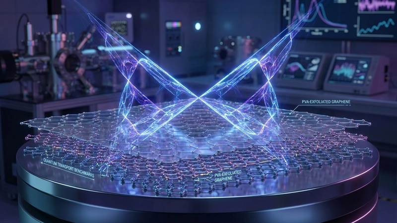
Hofstadter Butterfly and Quantum Transport Benchmarks in PVA-Exfoliated Graphene Heterostructures
Research conducted by: Takashi Taniguchi, Kevin Yager, Zihan Zhang, Davood Shahrjerdi, Suji Park, Pilkyung Moon, Kenji Watanabe, Moeid Jamalzadeh, Zhujun Huang
The scientific community owes a significant debt of gratitude to this dedicated team of researchers whose meticulous efforts have successfully challenged a long-standing paradigm in quantum materials science. Their collaborative work across multiple disciplines has not only illuminated the fundamental physics of moiré superlattices but has also provided a pragmatic roadmap for the scalable fabrication of high-purity quantum devices. By rigorously benchmarking polymer-exposed graphene heterostructures, they have opened new avenues for technological advancement that will undoubtedly influence the next generation of electronic and optoelectronic systems.
For over a decade, the fabrication of van der Waals heterostructures has been governed by a strict, almost dogmatic principle: polymers are the enemy of quantum purity. The delicate nature of emergent quantum phenomena in two-dimensional materials demands an environment free from disorder, and conventional wisdom has dictated that any exposure to organic polymers during the exfoliation and transfer processes inevitably introduces scattering centers, charge puddles, and structural impurities. This assumption has forced researchers into a frustrating compromise, pitting the scalable, high-yield advantages of polymer-assisted assembly against the pristine, low-disorder requirements of advanced quantum transport experiments. However, a paradigm-shifting study has now emerged to dismantle this assumption. By leveraging polyvinyl alcohol as an exfoliation medium and employing elevated-temperature lamination for hexagonal boron nitride encapsulation, researchers have demonstrated that polymer-exposed graphene can not only achieve foundational transport metrics but can also satisfy the most demanding quantum benchmarks known to solid-state physics. This article delves deep into the methodology, the physics, and the profound implications of achieving the Hofstadter butterfly spectrum in polymer-assisted graphene heterostructures.
The Persistent Polymer Problem in Quantum Material Fabrication
The journey to isolate and manipulate two-dimensional materials has always been fraught with microscopic hazards. When Andre Geim and Konstantin Novoselov first isolated graphene using the mechanical cleavage method—famously known as the scotch tape technique—they established a standard for material purity that has been difficult to scale. As the field evolved from studying single layers to stacking multiple two-dimensional crystals into complex van der Waals heterostructures, the need for precise, deterministic transfer methods became paramount. To pick up and place atomically thin layers of graphene, hexagonal boron nitride, and transition metal dichalcogenides, scientists turned to polymer stamps. Polymethyl methacrylate, polydimethylsiloxane, and polycarbonate became the workhorses of the nanofabrication laboratory.
Despite their utility, these polymers carry a significant drawback. When a polymer is dissolved or dissolved away after the transfer process, it rarely leaves the surface entirely clean. Hydrocarbon residues cling to the graphene lattice, acting as localized charge scatterers. In the realm of classical electronics, a small amount of residue might simply reduce the carrier mobility slightly, perhaps increasing the sheet resistance. But in the realm of quantum transport, where electrons are expected to travel ballistically over micrometers and exhibit delicate phase coherence, these residues are catastrophic. They create a fluctuating electrostatic potential landscape—often referred to as charge puddles—that destroys the fragile quantum states required for observing fractional quantum Hall effects, superconductivity, or correlated insulator states.
Consequently, the pursuit of the highest quality devices has historically driven researchers toward completely polymer-free transfer techniques. These methods, while yielding spectacularly clean devices, are notoriously difficult, time-consuming, and prone to low yield. They are artisanal processes, unsuited for the rapid prototyping or eventual commercialization of quantum technologies. The prevailing narrative has thus remained fixed: if you want scalable fabrication, you must sacrifice quantum purity; if you want quantum purity, you must abandon scalable polymer processing. The new research under discussion shatters this dichotomy by proving that not all polymers, and not all transfer processes, are created equal.
Polyvinyl Alcohol Exfoliation and Elevated Temperature Lamination
To circumvent the limitations of traditional polymer residues, the research team turned to polyvinyl alcohol, commonly abbreviated as PVA. Unlike the more aggressively adhesive polymers conventionally used in dry transfer methods, PVA is a water-soluble synthetic polymer that offers a unique combination of mechanical flexibility and chemical benignity. The researchers utilized PVA to assist in the mechanical exfoliation of graphene, capitalizing on its ability to yield large-area flakes without subjecting the delicate carbon lattice to harsh chemical solvents during the removal phase. Because PVA can be dissolved in water, the dissolution process is inherently gentler, minimizing the chemical bonding between the residue and the graphene surface.
However, the use of PVA alone is not sufficient to guarantee the pristine environment required for quantum transport. The true innovation lies in the subsequent encapsulation process. Two-dimensional materials are incredibly sensitive to their environment; even a perfectly clean graphene sheet will suffer from degraded mobility if placed directly on a standard silicon dioxide substrate due to trapped charges and surface roughness. To protect the graphene, it must be sandwiched between layers of hexagonal boron nitride, an insulating isomorph of graphite that provides an atomically flat, charge-neutral substrate and top cover.
The critical step introduced by the researchers is elevated-temperature lamination. During the assembly of the van der Waals heterostructure, the layers are brought into contact while being subjected to carefully controlled, high temperatures. This thermal energy serves a dual purpose. First, it increases the mobility of any microscopic contaminants or residual PVA molecules caught between the layers, allowing the intrinsic van der Waals forces to squeeze these impurities out into localized blister-like pockets, leaving vast expanses of the interface atomically clean. This self-cleansing mechanism is a well-documented phenomenon in two-dimensional material assembly, but its application to PVA-exfoliated graphene at specific elevated temperatures ensures a level of structural integrity previously thought impossible for polymer-exposed samples. Second, the heat promotes optimal conformal adhesion between the graphene and the hexagonal boron nitride, smoothing out microscopic wrinkles and ensuring a uniform dielectric environment across the entire device area.
Surpassing Foundational Metrics to Achieve Ballistic Transport
When evaluating the quality of a graphene device, the first line of inquiry typically involves foundational transport metrics: carrier mobility and charge inhomogeneity. Carrier mobility measures how quickly an electron can move through the material under an applied electric field, while charge inhomogeneity quantifies the spatial variation of the charge carrier density, essentially mapping the severity of the charge puddles mentioned earlier. Historically, polymer-exposed graphene devices have exhibited moderate mobilities and high charge inhomogeneity, relegating them to the realm of basic proof-of-concept experiments rather than rigorous quantum exploration.
The heterostructures fabricated using the PVA-assisted, high-temperature lamination method tell a vastly different story. Upon cooling these devices to cryogenic temperatures, the researchers recorded ultra-high carrier mobilities that rival those of the most meticulously crafted polymer-free devices. The electrons in these PVA-exposed samples streak across the lattice with minimal impedance, indicating that the traditional scattering mechanisms associated with polymer residue have been effectively neutralized or localized away from the active transport channels.
Furthermore, the devices exhibit ballistic transport over micrometer scales. In a ballistic transport regime, the mean free path of the charge carriers exceeds the physical dimensions of the device channel. This means that electrons travel from the source electrode to the drain electrode without experiencing a single scattering event. Observing ballistic transport is a monumental achievement for any graphene device, as it requires an almost perfect crystalline lattice and an exceptionally clean dielectric environment. The fact that this regime was accessed in a device assembled with the aid of a polymer definitively proves that PVA exposure, when coupled with the correct fabrication protocols, does not inherently compromise the structural or electronic integrity of the graphene. The charge inhomogeneity was found to be vanishingly small, confirming that the electrostatic potential landscape is flat and uniform, a prerequisite for the more advanced quantum phenomena to come.
Quantum Scattering Times and the Equivalence to Polymer Free Devices
While high mobility and ballistic transport are excellent indicators of device quality, they do not tell the whole story. To truly benchmark the quantum integrity of a two-dimensional electron system, researchers must investigate the quantum scattering time. Unlike the classical scattering time, which governs the overall resistivity and mobility by measuring momentum-relaxing collisions, the quantum scattering time is sensitive to all scattering events, including small-angle scattering that alters the phase of the electron wave function without significantly changing its momentum. It is a much more stringent metric; a device can have a high classical mobility but a low quantum scattering time if it is plagued by long-range impurities.
The quantum scattering time is typically extracted by analyzing Shubnikov-de Haas oscillations. When a magnetic field is applied perpendicular to the graphene plane, the continuous density of states splits into discrete, highly degenerate energy levels known as Landau levels. As the magnetic field or the charge carrier density is swept, these Landau levels cross the Fermi energy, resulting in periodic oscillations in the longitudinal resistance. By studying the amplitude of these oscillations as a function of the magnetic field and temperature, researchers can calculate the Dingle temperature, which is inversely proportional to the quantum scattering time.
In the PVA-exfoliated heterostructures, the Shubnikov-de Haas oscillations emerge at remarkably low magnetic fields, a direct consequence of low disorder. The subsequent extraction of the quantum scattering times yielded values that are virtually indistinguishable from the best polymer-free devices reported in the literature. This equivalence is the crux of the researchers argument. It demonstrates mathematically and experimentally that the phase coherence of the electrons in the PVA-exposed graphene is completely preserved. The subtle, long-range Coulomb scattering typically induced by polymer residues is conspicuously absent. By achieving these comparable quantum scattering times, the researchers have elevated polymer-assisted fabrication from a mere convenience to a scientifically rigorous methodology capable of supporting phase-coherent quantum experiments.
The Ultimate Test Exploring the Hofstadter Butterfly Spectrum
To put the final nail in the coffin of the polymer-residue stigma, the researchers subjected their devices to the most demanding quantum transport benchmark conceivable: the observation of the Hofstadter butterfly spectrum. Predicted by Douglas Hofstadter in 1976, this spectrum is a mesmerizing, fractal energy structure that emerges when electrons are subjected to two competing periodic potentials. In the context of graphene, the first periodic potential is provided by the crystalline lattice itself, or more specifically, by a moiré superlattice. When graphene is placed on hexagonal boron nitride with a slight rotational misalignment, the lattice mismatch and the twist angle create a larger, secondary periodic structure called a moiré pattern.
The second periodic potential is introduced by applying a strong perpendicular magnetic field. Quantum mechanics dictates that magnetic flux can only penetrate the lattice in discrete packets called flux quanta. The Hofstadter butterfly emerges when the magnetic flux penetrating a single moiré unit cell is comparable to the fundamental magnetic flux quantum. Because the moiré unit cell is much larger than the atomic unit cell, this condition can be met at experimentally accessible magnetic fields, typically between ten and thirty Tesla. The resulting energy spectrum is highly complex, recursive, and exquisitely sensitive to any spatial disorder.
If the interlayer coupling between the graphene and the hexagonal boron nitride is not perfectly uniform across the entire device—if there are microscopic bubbles, trapped polymer residues, or variations in the twist angle—the delicate fractal gaps of the Hofstadter butterfly will be smeared out and destroyed. It requires a vast area of pristine, homogeneously coupled material to manifest.
Astoundingly, the moiré superlattices fabricated from the PVA-exposed graphene clearly exhibited the Hofstadter butterfly spectra. Through high-resolution magnetotransport measurements, the researchers mapped out the intricate fan diagrams characteristic of the fractal energy states. The observation of primary and secondary Dirac points, along with the intricate crossing of Landau levels originating from these different points in the moiré Brillouin zone, confirms beyond a shadow of a doubt that the interlayer coupling is spatially uniform. The elevated-temperature lamination successfully expelled any residual PVA from the active area, allowing the graphene and boron nitride lattices to interact exactly as theoretical models predict. This achievement represents the ultimate vindication of the PVA-assisted methodology.
Bridging the Gap Between Scalable Fabrication and Quantum Transport
The successful observation of the Hofstadter butterfly in a polymer-exposed device is much more than a niche victory for condensed matter physicists; it represents a critical bridge between laboratory curiosity and scalable technological application. The field of twistronics, which explores the profound changes in electronic properties resulting from twisting layers of two-dimensional materials, relies heavily on the reliable fabrication of moiré superlattices. Phenomena such as magic-angle superconductivity, correlated insulators, and orbital magnetism require the utmost precision and purity.
Until now, the necessity of using polymer-free methods to achieve these states has severely bottlenecked the progress of twistronics. Researchers spend weeks fabricating a single viable device, limiting the pace of discovery and rendering statistical analysis nearly impossible. By proving that PVA-assisted exfoliation combined with elevated-temperature lamination can produce devices capable of hosting these highly fragile emergent phenomena, this research significantly relaxes the strict trade-off between scalability and purity.
Laboratories around the world can now adopt these polymer-assisted techniques with confidence, knowing that they are not sacrificing the fundamental integrity of the electronic system. This democratization of high-quality device fabrication will likely accelerate the discovery of new quantum phases and facilitate the rapid prototyping of novel quantum electronic components, such as highly sensitive magnetic field sensors, topological quantum computing architectures, and advanced optoelectronic modulators. The ability to utilize polymers for their mechanical advantages while mitigating their chemical drawbacks is a monumental leap forward for materials engineering.
Future Outlook for Engineered Residue Removal Protocols
While the current study focuses specifically on polyvinyl alcohol and elevated-temperature lamination, its broader implications extend to the entire philosophy of van der Waals heterostructure assembly. The results strongly motivate the further development of polymer-assisted assembly techniques coupled with engineered residue-removal protocols. PVA has proven its worth, but it is just one of many potential transfer mediums. The realization that thermal and mechanical manipulation during the lamination process can effectively isolate and neutralize polymer residues opens the door for exploring other sacrificial layers and adhesives.
Future research will likely focus on optimizing the temperature, pressure, and atmospheric conditions during the lamination phase to maximize the self-cleansing effect. Additionally, the integration of targeted solvent baths, ultraviolet ozone treatments, or remote plasma cleaning steps—carefully calibrated to avoid damaging the underlying crystal lattice—could further enhance the purity of polymer-exposed devices. The goal is no longer to avoid polymers entirely, but to design smart polymers and smart assembly protocols that work in tandem to produce pristine quantum environments.
As the demand for complex, multi-layered van der Waals heterostructures grows, the reliance on scalable transfer techniques will only increase. This pioneering research provides the foundational evidence that we do not have to choose between mass production and quantum perfection. By understanding and controlling the interplay between polymer chemistry, thermal dynamics, and crystalline interfaces, the scientific community is well on its way to unlocking the full technological potential of two-dimensional materials.
Frequently Asked Questions
Question: Why is polymer exposure usually considered bad for graphene devices?
Answer: Polymer exposure is typically considered detrimental because the organic molecules used in the transfer and exfoliation processes often leave behind microscopic hydrocarbon residues on the surface of the graphene. These residues act as localized scattering centers and create uneven electrostatic potentials, known as charge puddles. This disorder disrupts the smooth flow of electrons, severely reducing carrier mobility and destroying the delicate phase coherence required to observe advanced quantum mechanical phenomena.
Question: What makes polyvinyl alcohol different from other polymers used in these processes?
Answer: Polyvinyl alcohol is unique because it is a water-soluble synthetic polymer. Unlike traditional transfer polymers such as polymethyl methacrylate or polydimethylsiloxane, which require harsh chemical solvents like acetone or chloroform for removal, polyvinyl alcohol can be dissolved gently in water. This gentle dissolution process reduces the likelihood of strong chemical bonds forming between the polymer residue and the graphene lattice, resulting in a significantly cleaner initial surface before the encapsulation step.
Question: How does elevated-temperature lamination improve the quality of the device?
Answer: Elevated-temperature lamination applies thermal energy while the layers of the van der Waals heterostructure are being pressed together. This heat increases the mobility of any remaining microscopic contaminants or trapped air bubbles. The intrinsic van der Waals forces between the atomically flat layers then act to squeeze these impurities out of the main interface, pushing them into isolated pockets. Furthermore, the heat ensures better conformal adhesion, smoothing out wrinkles and creating a highly uniform dielectric environment.
Question: What is a quantum scattering time and why is it important here?
Answer: The quantum scattering time is a highly sensitive metric that measures the time between any scattering events an electron experiences, including those that only alter the phase of its wave function without changing its momentum. It is a much stricter measure of device purity than standard carrier mobility. Achieving quantum scattering times equivalent to those of polymer-free devices proves that the polyvinyl alcohol process successfully eliminates the subtle, long-range disorder that typically ruins quantum coherence in polymer-exposed samples.
Question: What does the observation of the Hofstadter butterfly spectrum prove?
Answer: The Hofstadter butterfly spectrum is a highly complex, fractal energy pattern that only emerges when electrons are subjected to a perfectly uniform periodic potential from a moiré superlattice and a strong magnetic field. Its observation is the ultimate test of device quality because any spatial variation in the interlayer coupling, twist angle, or localized disorder will immediately destroy the delicate fractal gaps. Seeing this spectrum definitively proves that the entire device area is exceptionally clean and homogeneously coupled, vindicating the polymer-assisted fabrication method.
Conclusion
The persistent belief that polymer exposure irrevocably compromises the quantum integrity of van der Waals heterostructures has been a significant bottleneck in the advancement of two-dimensional materials research. Through rigorous benchmarking and the successful observation of the highly fragile Hofstadter butterfly spectrum, the research team has conclusively demonstrated that polyvinyl alcohol-assisted exfoliation, when paired with elevated-temperature lamination, produces graphene devices of unparalleled quality. These heterostructures not only exhibit ultra-high mobility and ballistic transport but also boast quantum scattering times that match the most meticulously crafted polymer-free devices. By proving that spatially uniform interlayer coupling can be achieved in polymer-exposed samples, this study bridges the critical gap between scalable device fabrication and low-disorder quantum transport. It provides a robust, accessible methodology for researchers worldwide, ensuring that the exploration of complex moiré physics and the development of next-generation quantum technologies will no longer be hindered by the limitations of artisanal, low-yield assembly techniques. The future of twistronics and quantum materials engineering looks brighter, and significantly more scalable, than ever before.
Evaluate Our Quality
Serious about B2B integration? Test our premium Pulsed Electrical Resistive Carbon Heating turbostratic graphene in your lab. 100g sample packs available now.