Breakthrough in Flexible EMI Shielding: Silver-Modified Picosecond Laser-Induced Graphene
Research conducted by: Xiuqing Hao, Kewei Fu, Simin Chen, J Z Zhang, Guozheng Zhong, Ping Chen, Jie Zhou. This brilliant team of researchers has pioneered a transformative approach to electromagnetic compatibility, presenting their findings in a comprehensive study that bridges the critical gap between flexible electronics and robust electromagnetic interference shielding. Their meticulous work details the synthesis and application of flexible picosecond laser-induced graphene films modified with silver nanoparticles, offering a scalable and highly efficient solution for the next generation of wearable and integrated electronic devices. By addressing the inherent limitations of standard laser-induced graphene, their research provides a foundational blueprint for developing advanced, flexible metamaterial absorbers capable of operating over broad frequency ranges. Their dedication to unravelling the complex mechanisms behind laser processing and material science has resulted in a unified platform that will significantly impact the telecommunications, aerospace, and consumer electronics industries.
The proliferation of highly integrated electronic devices has brought about a silent but pervasive form of pollution known as electromagnetic interference. As smartphones, wearable health monitors, autonomous vehicle sensors, and flexible displays become increasingly compact and powerful, the electromagnetic signals they emit and receive can cross paths. This invisible cross-talk leads to severe signal degradation, catastrophic data loss, and even critical hardware malfunction. Traditional electromagnetic shielding materials, predominantly rigid metal plates, conductive foams, and heavy metallic foils, are fundamentally incompatible with the emerging paradigm of flexible and wearable electronics. They add unwanted weight, lack conformability, and are highly prone to mechanical failure under repeated bending and stretching. Consequently, the scientific community has been on a relentless quest to discover materials that are lightweight, highly conductive, mechanically robust, and capable of absorbing or reflecting stray electromagnetic waves. Laser-induced graphene has emerged as a highly promising candidate to fulfill these demanding criteria. By simply irradiating a polyimide film with a laser, the polymer is photothermally and photochemically converted into a three-dimensional, porous graphene network. This technique is completely maskless, highly scalable, and customizable for roll-to-roll manufacturing. However, utilizing picosecond lasers to induce this transformation introduces specific, complex challenges that have historically bottlenecked its commercial application.
Overcoming the Limitations of Picosecond Laser-Induced Graphene
While femtosecond and continuous-wave carbon dioxide lasers have been extensively studied for graphene induction, picosecond lasers offer a unique balance of thermal and photochemical effects that make them highly attractive for industrial scaling. They provide extremely high peak power with a very short pulse duration, which minimizes the heat-affected zone and prevents damage to the underlying delicate flexible substrates. However, picosecond laser-induced graphene has historically suffered from significant microstructural drawbacks. The primary issue lies in limited microstructural continuity. The rapid ablation and intense localized heating caused by picosecond pulses often result in a fragmented, discontinuous graphene network. This fragmentation acts as a massive barrier to the smooth flow of electrons, impeding the high electrical conductivity that is a strict prerequisite for effective electromagnetic shielding.
Furthermore, researchers have faced restricted tunability of sheet resistance. In advanced electromagnetic applications, the ability to precisely tune the electrical resistance of the shielding material is critical for achieving perfect impedance matching. Impedance matching is a physical condition where the material is engineered to absorb incoming electromagnetic waves entirely, rather than reflecting them back into the environment and causing secondary interference. Previous attempts to construct flexible conductive networks using picosecond laser-induced graphene fell short because the resistance could not be reliably controlled over a functionally wide range. The material was either too resistive or too conductive, with very little middle ground.
The research team tackled this bottleneck head-on by systematically investigating the fundamental formation mechanism of the graphene on polyimide substrates. They mapped out a clear, predictable, and highly detailed correlation between the laser processing parameters, the resulting microstructural evolution of the carbon lattice, and the final electrical resistance of the films. By meticulously fine-tuning the laser power, the scanning speed across the substrate, and the pulse frequency, they unlocked a broad and trend-governed tuning capability. This breakthrough allowed them to manipulate the sheet resistance across a massive and highly useful range of ten to one thousand two hundred ohms per square. This level of precise control is unprecedented in picosecond laser applications and serves as the absolute foundation for the advanced electromagnetic functional properties demonstrated later in their comprehensive study.
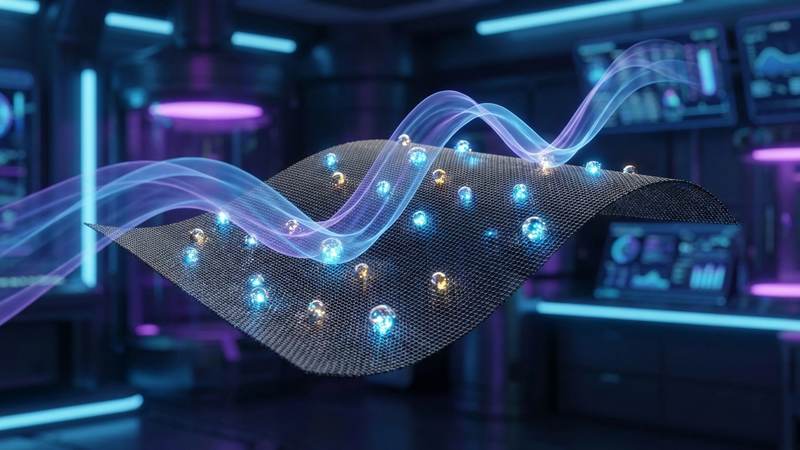
The Integration of Silver Nanoparticles for Enhanced Conductivity
Achieving highly tunable resistance was only the first step in creating a viable commercial material. To elevate the shielding effectiveness to the stringent levels required by modern electronics, the researchers needed to physically bridge the microscopic gaps and discontinuous fault lines within the picosecond laser-induced graphene network. Their ingenious solution was the introduction of silver nanoparticles. Silver is globally renowned for its exceptional electrical conductivity, but successfully integrating rigid metal nanoparticles into a flexible, porous graphene matrix without destroying its mechanical flexibility is a profound metallurgical and chemical challenge.
The team achieved this integration through a highly efficient, elegant process known as laser-assisted in situ reduction. Instead of using complex, toxic chemical baths or energy-intensive high-temperature furnaces, they utilized the precise energy of the picosecond laser itself to accomplish two tasks simultaneously. As the laser converts the polyimide polymer into a graphene structure, it also provides the exact activation energy required to reduce silver precursor compounds directly into pure, crystalline silver nanoparticles within the newly formed porous architecture. This one-step, in situ method ensures that the silver nanoparticles are exceptionally uniformly distributed and intimately bonded to the edges and basal planes of the graphene flakes.
The result is a highly advanced flexible composite conductive network. The silver nanoparticles act as highly efficient conductive bridges, effectively healing the microstructural discontinuities inherent in the original picosecond laser-induced graphene. Electrons can now flow unimpeded across the material, utilizing the silver nodes to bypass any structural gaps. Crucially, this laser-assisted integration preserves the intrinsic, highly porous architecture of the graphene. This porosity is not a structural defect; rather, it is a vital engineered feature that drastically lowers the overall density of the material, keeping it incredibly lightweight. Furthermore, the porous network provides a massive internal surface area that facilitates multiple internal scattering and reflections of electromagnetic waves. As the waves bounce around inside the microscopic voids, their energy is rapidly depleted, thereby massively enhancing the overall absorption capabilities of the composite material.
Achieving Unprecedented Electromagnetic Shielding Effectiveness
The true test of this newly developed composite material lies in its quantifiable ability to block electromagnetic interference. Electromagnetic shielding effectiveness is universally measured in decibels, a logarithmic scale that denotes the ratio of incident energy to transmitted energy. The transition from pure picosecond laser-induced graphene to the silver-modified composite version yielded dramatic, paradigm-shifting results. The pristine, unmodified graphene films exhibited a baseline shielding effectiveness of approximately nineteen point five decibels. While this is acceptable for low-end, low-frequency applications, it falls woefully short of the stringent requirements demanded by modern aerospace, military, and high-frequency consumer electronics.
With the successful introduction of the silver nanoparticles, the shielding effectiveness skyrocketed to approximately thirty decibels. To put this logarithmic leap into perspective, a shielding effectiveness of thirty decibels means that exactly ninety-nine point nine percent of the incident electromagnetic radiation is blocked by the material. Only a negligible fraction of a percent manages to pass through. This exponential leap in performance is directly attributed to two primary physical mechanisms working in perfect synergy. First, the enhanced electron transport continuity provided by the silver bridges allows the composite to highly reflect and rapidly dissipate the electrical component of the incoming electromagnetic waves through conduction loss.
Second, the myriad of interfaces between the crystalline silver nanoparticles and the carbonaceous graphene sheets introduces incredibly strong interfacial polarization effects. When an alternating electromagnetic wave strikes these heterogeneous interfaces, localized electrical charges accumulate, creating microscopic dipoles that oscillate rapidly with the high frequency of the incoming wave. This intense oscillation acts as a friction mechanism at the atomic level, converting the dangerous electromagnetic energy into minute, harmless amounts of heat. This heat is then safely and rapidly dissipated across the highly thermally conductive graphene network. The flawless synergy between the highly conductive macroscopic network and the billions of microscopic polarization centers makes this composite an incredibly formidable, almost impenetrable barrier against electromagnetic pollution.
Mechanical Durability and the Flexibility Factor
The fundamental, non-negotiable requirement for materials intended for flexible electronics is, unsurprisingly, robust mechanical flexibility. A remarkably high shielding effectiveness is rendered completely useless if the material cracks, flakes, delaminates, or loses its electrical conductivity the very moment it is bent, twisted, or folded. Traditional rigid metal shields fail precisely because of mechanical fatigue and stress fractures. The research team rigorously tested the mechanical durability of their silver-modified picosecond laser-induced graphene films to ensure they could easily withstand the punishing physical demands of real-world wearable applications and dynamic device hinges.
The polyimide substrate itself is renowned for being highly flexible, which is why it is the industry standard for flexible printed circuits. However, the critical question was whether the newly integrated graphene and silver network could maintain its structural and electrical integrity under severe mechanical stress. To prove this, the composite films were subjected to a highly punishing regimen of cyclic bending tests using automated machinery. After enduring five hundred extreme bending cycles at tight radiuses, the composite material miraculously maintained approximately eighty-three percent of its initial electromagnetic shielding performance.
This remarkable retention rate strongly indicates that the conductive pathways formed by the silver nanoparticles and the graphene flakes are highly resilient and structurally sound. The porous nature of the graphene actually plays a crucial, protective role here. The microscopic voids within the structure act as tiny crumple zones that absorb and dissipate mechanical stress, effectively preventing the nucleation and propagation of macroscopic cracks that would otherwise sever the electrical connections. This robust mechanical flexibility ensures that the electromagnetic functional properties remain highly stable even when the material is permanently integrated into the folding hinges of next-generation smartphones, embedded deep within the woven fabrics of smart athletic clothing, or wrapped tightly around the irregular, moving contours of advanced robotic joints.
Unprecedented Broadband Electromagnetic Absorption Capabilities
Shielding against electromagnetic interference often involves a complex combination of reflection and absorption. While simply reflecting waves away from a sensitive electronic component is helpful, it is often a flawed strategy because it merely bounces the high-energy interference into another direction, potentially causing severe problems for adjacent sensitive devices in a densely packed system. The ultimate, highly sought-after goal in electromagnetic compatibility engineering is to absorb the stray waves entirely, completely neutralizing them by converting their electromagnetic energy into harmless thermal energy. Building upon the highly tunable sheet resistance of their newly developed material, the researchers took their work a step further and designed a flexible multilayer metamaterial absorber.
Metamaterials are artificially engineered structures designed to interact with electromagnetic waves in highly specific ways that natural, unpatterned materials simply cannot achieve. By exploiting the ultra-precise patterning capability of the picosecond laser, the team was able to etch exact, mathematical geometric shapes into the graphene films. These meticulously patterned layers were then stacked with specific dielectric spacers to create a complex structure that perfectly matches the impedance of free space. When the impedance of the material matches the impedance of the air, electromagnetic waves can enter the material seamlessly without bouncing off the front surface. Once trapped inside this metamaterial architecture, the waves are rapidly attenuated and destroyed by the silver-graphene composite network.
The absorption measurements resulting from this multilayer metamaterial design were nothing short of spectacular. The metamaterial achieved a broadband and highly efficient electromagnetic absorption profile with a massive bandwidth of twelve point nine gigahertz. This effective absorption covered an operational frequency range stretching all the way from five point one gigahertz up to eighteen gigahertz. This incredibly broad spectrum is highly significant because it encompasses the most critical and heavily utilized frequencies used in modern telecommunications, including advanced Wi-Fi networks, Bluetooth protocols, satellite communications, marine radar, and the rapidly expanding fifth-generation cellular networks. By efficiently capturing and permanently neutralizing such a wide array of frequencies, this metamaterial platform proves its immense versatility and immediate readiness for deployment in next-generation telecommunications infrastructure and advanced stealth technologies.
Frequently Asked Questions
Question: What is picosecond laser-induced graphene and how is it made?
Answer: Picosecond laser-induced graphene is a highly conductive, three-dimensional, porous carbon material. It is created by irradiating a specific carbon-rich polymer, most commonly polyimide, with a picosecond pulsed laser. The intense, ultra-short bursts of laser energy instantly break the chemical bonds within the polymer matrix and force the remaining carbon atoms to rearrange themselves into a highly structured, conductive graphene lattice. Because the laser pulses are in the picosecond range, the process generates very little excess heat, protecting the surrounding material.
Question: Why are silver nanoparticles specifically added to the graphene structure?
Answer: Silver nanoparticles are intentionally added to act as highly efficient conductive bridges across the microscopic gaps in the laser-induced graphene network. Because picosecond lasers can sometimes cause fragmentation and discontinuity in the carbon lattice, the highly conductive silver heals these faults. This ensures smooth, continuous electron transport across the entire material, which drastically improves the overall electrical conductivity and massively boosts the material's electromagnetic shielding effectiveness.
Question: How is the sheet resistance of this composite material controlled during manufacturing?
Answer: The sheet resistance is meticulously controlled by precisely adjusting the fundamental laser processing parameters, which include the laser's power output, the scanning speed of the beam across the substrate, and the pulse repetition frequency. By fine-tuning these specific settings, researchers can exactingly control the degree of graphitization and the density of the porous network. This level of control allows them to reliably tune the electrical resistance anywhere from a highly conductive ten ohms per square to a highly resistive one thousand two hundred ohms per square.
Question: What does a shielding effectiveness of thirty decibels actually mean in practical terms?
Answer: Shielding effectiveness is measured on a logarithmic scale to describe how well a material blocks electromagnetic radiation. A value of thirty decibels means that the material attenuates the incoming electromagnetic wave by a massive factor of one thousand. In practical, real-world terms, this signifies that exactly ninety-nine point nine percent of the harmful electromagnetic energy is successfully blocked and prevented from passing through the material, providing exceptional protection for sensitive electronics.
Question: Why is mechanical flexibility such an important factor for modern electromagnetic shielding?
Answer: As modern electronic devices rapidly evolve to become wearable, foldable, and seamlessly integrated into non-flat surfaces, traditional rigid metal shields are no longer viable because they snap and break under repeated physical stress. Flexible shielding materials, like the silver-modified graphene discussed in this study, can easily conform to complex, moving shapes and withstand thousands of extreme bending cycles without losing their vital conductive properties. This makes them absolutely essential for the physical design of modern and future electronic devices.
Conclusion
The meticulous research and innovative engineering demonstrated in this comprehensive study mark a truly significant milestone in the critical field of electromagnetic compatibility. By systematically isolating and addressing the inherent limitations of picosecond laser-induced graphene, and ingeniously integrating silver nanoparticles via a highly efficient laser-assisted in situ reduction process, the research team has unlocked a completely new tier of material performance. Their flexible multilayer metamaterial absorber not only delivers exceptional, world-class electromagnetic shielding effectiveness but also provides unparalleled, broadband wave absorption across the most critical and heavily congested modern communication frequencies.
The unique ability to precisely tune the electrical properties of the material during a single-step manufacturing process, combined with its robust, proven mechanical flexibility, establishes a unified and highly scalable platform for future industrial applications. As the global consumer and military demand for increasingly compact, flexible, and immensely powerful electronic devices continues to surge exponentially, the threat of electromagnetic interference will only grow. The advanced composite materials developed in this groundbreaking work will undoubtedly play a crucial, foundational role in ensuring that our increasingly interconnected world operates smoothly, efficiently, and entirely free from the disruptive, invisible chaos of electromagnetic pollution. This research paves the way for safer, faster, and more reliable flexible electronics for decades to come.
Evaluate Our Quality
Serious about B2B integration? Test our premium Pulsed Electrical Resistive Carbon Heating turbostratic graphene in your lab. 100g sample packs available now.