Unveiling the Potential Landscape of Bilayer Graphene Quantum Dots Through COMSOL Electrostatic Simulation
Research conducted by: Ho Yeon Yoo
This groundbreaking investigation provides a comprehensive look into the electrostatic environments of advanced nanoelectronic structures. Yoo and the associated research team have meticulously modeled the potential landscape of an encapsulated device, shedding light on the intricate behaviors of charge carriers confined within two-dimensional materials. Their work bridges the gap between theoretical electrostatics and observable quantum phenomena, offering critical insights into how we might control quantum states for future computing architectures. By utilizing advanced computational tools to simulate the exact geometric and dielectric properties of the device, this research clarifies the underlying mechanisms that govern charge confinement, edge-state activation, and the dynamic reconstruction of quantum-dot networks.
The pursuit of scalable and coherent quantum computing architectures has driven materials scientists and condensed matter physicists to explore a vast array of solid-state platforms. Among these, carbon-based nanomaterials have emerged as highly promising candidates due to their weak spin-orbit coupling and sparse concentration of nuclear spins, both of which are critical factors in mitigating qubit decoherence. While single-layer graphene offers extraordinary carrier mobility, its lack of an inherent bandgap presents significant challenges for electrostatic confinement. To create a quantum dot in single-layer graphene, researchers historically had to rely on physical etching to shape the material into nanoribbons or islands. Unfortunately, physical etching introduces structural disorder, edge roughness, and localized defect states that act as charge traps, severely degrading device performance and predictability.
Bilayer graphene, however, circumvents this fundamental limitation. When subjected to a transverse electric field, bilayer graphene develops a tunable bandgap, allowing researchers to confine charge carriers using purely electrostatic means. This paradigm shift enables the creation of highly pristine, electrostatically defined quantum dots without the need for destructive physical patterning. The research modeled in these COMSOL simulations captures the precise electrostatic landscape required to achieve such confinement, taking into account the complex interplay between multiple gate electrodes, dielectric encapsulation layers, and the unique electronic band structure of the bilayer graphene channel itself.
The Architecture of Hexagonal Boron Nitride Encapsulation
To fully appreciate the significance of the electrostatic simulations, one must first understand the physical architecture of the device being modeled. The platform relies on a sophisticated heterostructure where the bilayer graphene channel is sandwiched between two crystalline layers of hexagonal boron nitride. This encapsulation technique is paramount for realizing high-quality quantum transport devices. Hexagonal boron nitride is an isomorphic insulator to graphene, sharing a similar honeycomb lattice structure but possessing a large, wide bandgap. Crucially, it is atomically flat and free of dangling bonds, making it an ideal dielectric substrate and superstrate.
When bilayer graphene is placed directly on traditional substrates like silicon dioxide, it suffers from severe degradation of its electronic properties. The amorphous nature of silicon dioxide introduces surface roughness, while trapped charges and impurities within the oxide layer create a highly disordered local electrostatic environment. These random potential fluctuations, often referred to as electron puddles, can completely mask the delicate quantum phenomena researchers intend to study. By encapsulating the bilayer graphene in hexagonal boron nitride, the graphene is physically isolated from the deleterious effects of the surrounding environment. The resulting heterostructure exhibits carrier mobilities that are orders of magnitude higher than those of unencapsulated devices.
The COMSOL simulation files meticulously account for this encapsulated geometry. The dielectric constant of hexagonal boron nitride is explicitly defined within the finite element model, ensuring that the capacitive coupling between the gate electrodes and the bilayer graphene channel is accurately represented. The thickness of both the top and bottom hexagonal boron nitride flakes plays a critical role in screening the electrostatic fields and determining the ultimate shape of the confinement potential. By accurately modeling these dielectric layers, the simulation provides a realistic map of the electric field distribution, confirming that the encapsulation not only protects the graphene but also serves as a highly efficient medium for electrostatic gating.
Bilayer Graphene as an Advanced Quantum Dot Platform
The fundamental physics of bilayer graphene makes it an exceptionally versatile platform for quantum dot definition. In its natural state, Bernal-stacked bilayer graphene is a zero-gap semiconductor with parabolic valence and conduction bands that touch at the Dirac points. However, when a perpendicular electric field is applied across the two layers, the inversion symmetry of the lattice is broken. This symmetry breaking opens a bandgap that is directly proportional to the strength of the applied displacement field. This unique property is the cornerstone of electrostatic confinement in this material system.
In the modeled device, a global back gate and a set of local top gates work in tandem to manipulate this bandgap. The global back gate, typically separated from the device by a thick layer of silicon dioxide and the bottom hexagonal boron nitride flake, applies a uniform electric field across the entire bilayer graphene channel. Simultaneously, the top gates, which are patterned into specific geometries, apply localized electric fields. By carefully tuning the voltages applied to these various gates, researchers can independently control both the carrier density and the transverse displacement field at any given point within the channel.
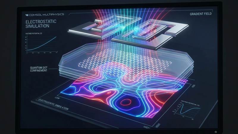
To create a quantum dot, the gate voltages are configured to open a wide bandgap in the regions surrounding the desired dot location, while the Fermi level is tuned into the gap, effectively rendering those regions insulating. In the central dot region, the local potential is adjusted to accumulate either electrons or holes, creating a tiny, conductive island completely surrounded by an electrostatically defined insulating barrier. The COMSOL simulations beautifully illustrate this process, solving Poisson's equation across the intricate three-dimensional geometry to reveal the exact spatial dimensions and depth of the resulting potential well. This electrostatic landscape defines the energy levels and orbital states of the confined charge carriers, dictating the ultimate quantum mechanical behavior of the dot.
The Role of COMSOL Multiphysics in Electrostatic Modeling
Understanding the precise electrostatic environment of a nanoscale device is a non-trivial challenge that requires sophisticated computational techniques. COMSOL Multiphysics is an industry-standard finite element analysis software that excels in solving coupled partial differential equations across complex geometries. In the context of this research, COMSOL is utilized to solve the electrostatic Poisson equation, which relates the electric potential distribution to the charge density and the spatial arrangement of dielectric materials.
The simulation model encompasses the entirety of the device geometry, including the global back gate, the bottom dielectric layers, the bilayer graphene channel, the top hexagonal boron nitride layer, and the intricately patterned split gates. Each domain within the model is assigned specific material properties, such as relative permittivity, to accurately reflect the physical device. The boundaries of the model are carefully defined with appropriate boundary conditions, ensuring that the simulated electric fields behave realistically at the edges of the computational domain.
One of the most critical aspects of the COMSOL simulation is its ability to handle the extreme aspect ratios inherent in two-dimensional material devices. The bilayer graphene channel is merely two atoms thick, yet it spans micrometers in the lateral dimensions. The finite element mesh must be intelligently designed to provide extremely high resolution in the immediate vicinity of the graphene layer and the gate edges, where the electric field gradients are steepest, while maintaining computational efficiency in the thicker dielectric regions. The output of these simulations is a high-resolution, three-dimensional map of the electrostatic potential landscape, providing researchers with an indispensable tool for visualizing the confinement barriers, calculating the lever arms of the various gates, and predicting the capacitive coupling between the quantum dot and its surrounding environment.
Split Gates and Local Electrostatic Offsets
The specific gate geometry employed in this device features a split-gate architecture, a design commonly used to create narrow, quasi-one-dimensional conduction channels or isolated zero-dimensional quantum dots. The split gates consist of metallic electrodes separated by a narrow gap, situated above the top hexagonal boron nitride layer. By applying a repelling voltage to these split gates, the charge carriers directly beneath them are depleted, funneling the remaining current through the narrow gap between the electrodes. Additional fine-tuning gates, often referred to as finger gates or plunger gates, can be placed within or across this gap to further compartmentalize the channel and define the isolated quantum dot.
The COMSOL simulations were specifically designed to examine how local electrostatic offsets under these split gates modify the confinement potential. In a perfectly ideal device, the electric field generated by a gate electrode would be perfectly uniform directly beneath it and drop to zero immediately outside its footprint. However, in reality, electrostatic fringing fields extend outward from the edges of the metallic gates, creating a smoothed, varying potential landscape rather than a sharp step function. Furthermore, structural imperfections, localized trapped charges in the dielectrics, or slight asymmetries in the gate fabrication can introduce local electrostatic offsets.
These offsets break the ideal symmetry of the confinement potential, warping the shape of the quantum dot and altering the height of the tunnel barriers that connect the dot to the source and drain reservoirs. The simulation files allow researchers to intentionally introduce these local offsets into the model and observe their effects in real-time. By systematically varying the simulated voltages and offset parameters, the research demonstrates how even minute changes in the local electrostatic environment can drastically shift the position of the potential minimum, change the spatial extent of the electron wavefunction, and alter the charging energy of the quantum dot. This detailed understanding is crucial for experimentalists attempting to tune the device into a regime where single-electron transport can be reliably observed and manipulated.
Edge-Dot Activation and the Potential Landscape
One of the most profound discoveries supported by these COMSOL simulations is the phenomenon of edge-dot activation. In a standard operational model, researchers focus entirely on the primary quantum dot defined in the center of the channel by the split gates and plunger gates. However, the physical edges of the bilayer graphene flake introduce a complex boundary condition that significantly alters the local electrostatics. At the physical edge of the crystal, the translational symmetry of the lattice is broken, and the dielectric environment abruptly changes from encapsulated graphene to the surrounding vacuum or polymer residue.
The simulations reveal that the electrostatic fringing fields from the split gates interact with the physical edges of the bilayer graphene channel to create unintended, localized potential minima. As the gate voltages are swept to tune the primary central dot, the local electrostatic offsets can deepen these potential wells at the channel edges, effectively activating additional, parasitic dot-like regions. These edge dots act as parallel conduction pathways or localized charge traps that couple capacitively and tunnel-mechanically to the primary central dot.
Understanding the activation of these edge dots is vital because they can severely complicate the transport spectroscopy of the device. When an experimentalist measures the conductance through the device, the presence of edge dots can manifest as overlapping Coulomb blockade diamonds, chaotic fluctuations in the current, or avoided crossings in the charge stability diagram. Without the spatial resolution provided by the COMSOL electrostatic simulations, identifying the physical origin of these complex signals would be nearly impossible. The simulations definitively link the local electrostatic offsets under the split gates to the formation of these edge-localized states, providing a clear electrostatic interpretation of the anomalous transport features observed in the associated manuscript.
Quantum-Dot-Network Reconstruction
The activation of edge dots alongside the primary central dot leads to a phenomenon described as quantum-dot-network reconstruction. Rather than behaving as a single, isolated quantum system, the device transforms into a complex network of multiple, coupled quantum dots. The spatial arrangement, capacitive coupling, and tunnel rates between the nodes in this network are entirely dictated by the highly tunable electrostatic potential landscape visualized in the COMSOL simulations.
As the voltages on the split gates and the global back gate are dynamically varied, the depths and spatial positions of both the central dot and the edge dots shift. This shifting alters the inter-dot coupling strengths. In one voltage regime, the central dot may be strongly coupled to the source and drain leads, while the edge dots remain empty and inactive. In another regime, the local electrostatic offsets might push the central dot out of resonance while simultaneously pulling an edge dot into the transport window, effectively shifting the active conduction path from the center of the channel to the periphery.
This dynamic reconfiguration of the active quantum states is what constitutes the reconstruction of the network. The COMSOL simulations provide a theoretical blueprint for this reconstruction, mapping out the precise voltage parameter space where these transitions occur. While unintentional network reconstruction can be a nuisance for experiments requiring a single, well-behaved qubit, a deep understanding of this process opens the door to advanced device functionalities. By deliberately designing the gate geometry to control the activation and coupling of edge dots, researchers could potentially exploit this network reconstruction to engineer tunable multi-qubit systems, simulate complex quantum impurity models, or route quantum information along dynamically defined pathways within the solid-state architecture.
Frequently Asked Questions
What is a bilayer graphene quantum dot?
A bilayer graphene quantum dot is a nanoscale region within a two-layer sheet of carbon atoms where charge carriers, such as electrons or holes, are confined in all three spatial dimensions. Unlike single-layer graphene, bilayer graphene can develop a bandgap when subjected to a perpendicular electric field. This allows researchers to use gate electrodes to create an insulating barrier around a specific central region, trapping a highly controllable number of charge carriers. These confined carriers exhibit quantized energy levels, much like electrons in a natural atom, making them excellent candidates for quantum computing qubits.
Why is hexagonal boron nitride used in these devices?
Hexagonal boron nitride is utilized as an encapsulation material because it provides an exceptionally clean and atomically flat environment for the bilayer graphene. Traditional oxide substrates possess rough surfaces and trapped chemical impurities that create random electrostatic fluctuations, which disrupt the delicate quantum states of the confined electrons. Hexagonal boron nitride shares a similar crystal lattice structure with graphene but acts as a wide-bandgap insulator. Sandwiching the graphene between layers of this material protects it from external contamination and smooths out the local electrostatic landscape, resulting in significantly higher carrier mobility and more stable quantum dot operation.
How does COMSOL simulation aid in quantum device design?
COMSOL simulation provides a rigorous mathematical framework for visualizing and calculating the invisible electric fields that dictate device behavior. By solving Poisson's equation across a three-dimensional model of the device, COMSOL generates a high-resolution map of the electrostatic potential landscape. This allows researchers to see exactly how the voltages applied to various microscopic gate electrodes interact with the dielectric layers to shape the confinement well of the quantum dot. It essentially acts as a virtual testing ground, enabling scientists to optimize gate geometries, predict capacitive coupling, and understand complex edge effects before committing to the expensive and time-consuming process of physical nanofabrication.
What are edge dots in the context of this research?
Edge dots are unintended, localized potential wells that form near the physical boundaries of the bilayer graphene channel. They are created by the complex interaction between the electrostatic fringing fields of the top gate electrodes and the abrupt termination of the graphene crystal lattice. The COMSOL simulations demonstrated that local electrostatic offsets can deepen these peripheral potential wells, causing them to trap charge carriers and act as secondary quantum dots. These edge dots can interfere with the operation of the primary central dot, but understanding their formation allows researchers to either mitigate their effects or potentially utilize them in more complex multi-dot architectures.
How does quantum-dot-network reconstruction impact quantum computing?
Quantum-dot-network reconstruction refers to the dynamic changing of the active charge transport pathways within the device as gate voltages are tuned, shifting dominance between central dots and edge dots. For basic quantum computing applications that require a single, isolated qubit, this reconstruction can cause decoherence and computational errors. However, if this phenomenon can be precisely mapped and controlled, as enabled by these detailed electrostatic simulations, it presents a unique opportunity. Controlled network reconstruction could allow physicists to dynamically wire and rewire connections between multiple qubits on the fly, paving the way for highly flexible, scalable, and reconfigurable quantum processing units.
Conclusion
The detailed COMSOL electrostatic simulations of the hexagonal boron nitride encapsulated bilayer graphene quantum-dot device represent a significant leap forward in our understanding of nanoscale charge confinement. By accurately modeling the complex interplay between the device geometry, dielectric layers, and localized gate voltages, this research illuminates the hidden electrostatic forces that govern quantum transport. The discovery and thorough characterization of edge-dot activation and the subsequent quantum-dot-network reconstruction provide crucial insights into the anomalous behaviors often observed in these advanced materials. Ultimately, these computational models serve as an indispensable roadmap, guiding experimental physicists toward the realization of cleaner, more reliable, and highly tunable bilayer graphene quantum devices that will form the backbone of next-generation solid-state quantum computing architectures.
Evaluate Our Quality
Serious about B2B integration? Test our premium Pulsed Electrical Resistive Carbon Heating turbostratic graphene in your lab. 100g sample packs available now.