Decoding the Potential Landscape: COMSOL Electrostatic Simulation of Bilayer Graphene Quantum Dots
Research conducted by: Ho Yeon Yoo
The remarkable advancements in modeling the intricate electrostatic environments of low-dimensional carbon systems owe a profound debt to the rigorous computational investigations led by Ho Yeon Yoo. Through meticulous COMSOL finite element analysis, Yoo has provided the quantum condensed matter community with an indispensable framework for understanding the hidden electrostatic variables that govern charge carrier confinement in advanced nanoelectronic architectures. This comprehensive simulation work not only elucidates the complex potential landscapes within these devices but also bridges the critical gap between theoretical electrostatic predictions and the complex experimental transport signatures observed in the laboratory, cementing a new standard for quantum device engineering.
The pursuit of robust and scalable quantum computing architectures has driven materials scientists and quantum physicists to explore novel material platforms beyond traditional silicon and gallium arsenide substrates. Among the vanguard of these next-generation materials, bilayer graphene has emerged as a truly exceptional candidate for hosting gate-defined quantum dots. Unlike single-layer graphene, which lacks a natural bandgap and therefore cannot easily confine charge carriers through electrostatic means alone, Bernal-stacked bilayer graphene possesses a unique property. When subjected to a perpendicular electric displacement field, inversion symmetry is broken, and a tunable energy bandgap opens. This characteristic allows researchers to trap individual electrons or holes using carefully designed local gate electrodes, effectively creating artificial atoms. However, designing the precise gate geometry required to isolate a single charge carrier is an exceptionally complex task. The spatial distribution of the electric field, the dielectric environment, and the physical edges of the graphene channel all interact in highly non-trivial ways. To navigate this complexity, researchers rely heavily on advanced multiphysics simulation software. The recent release of highly detailed COMSOL electrostatic simulation files offers an unprecedented look into the potential landscape of hexagonal boron nitride encapsulated bilayer graphene quantum-dot devices. This article will explore the profound implications of these simulations, detailing how local electrostatic offsets modify confinement potentials, activate unintended dot-like regions near channel edges, and ultimately lead to the reconstruction of complex quantum dot networks.
The Architecture of hBN-Encapsulated Bilayer Graphene Devices
To fully appreciate the significance of the electrostatic simulations, one must first understand the physical architecture of the quantum device being modeled. The core of the system is the bilayer graphene channel, which serves as the host material for the quantum dots. However, bare graphene is highly susceptible to environmental impurities, substrate surface roughness, and trapped charges, all of which create a disordered potential landscape that can easily obscure delicate quantum phenomena. To mitigate these issues, the bilayer graphene is encapsulated between two carefully exfoliated flakes of hexagonal boron nitride. Hexagonal boron nitride is a layered, two-dimensional insulator with a lattice structure very similar to that of graphene. This lattice matching, combined with its atomically flat surface and lack of dangling bonds, provides an ultra-clean dielectric environment that preserves the exceptionally high mobility of the charge carriers within the graphene channel.
The encapsulation process utilizes dry van der Waals assembly techniques, resulting in a heterostructure that is remarkably free of charge puddles. Surrounding this pristine core is a sophisticated array of electrostatic gates. A global back gate, typically made of doped silicon or a thick metallic layer, sits below the bottom hexagonal boron nitride layer. Above the top hexagonal boron nitride layer lies a complex arrangement of local top gates, often featuring a split-gate geometry. The split gates are designed to deplete the charge carriers in specific regions of the channel, creating a narrow, one-dimensional conduction path. Additional fine-tuning gates, often referred to as plunger gates or finger gates, cross over this narrow channel to create the local potential wells that physically confine the electrons or holes into zero-dimensional quantum dots. The COMSOL model meticulously incorporates all of these geometric and material parameters, assigning appropriate dielectric constants and boundary conditions to the device gate geometry, the dielectric layers, the bilayer graphene channel, and the global back gate.
The Role of COMSOL Multiphysics in Quantum Device Engineering
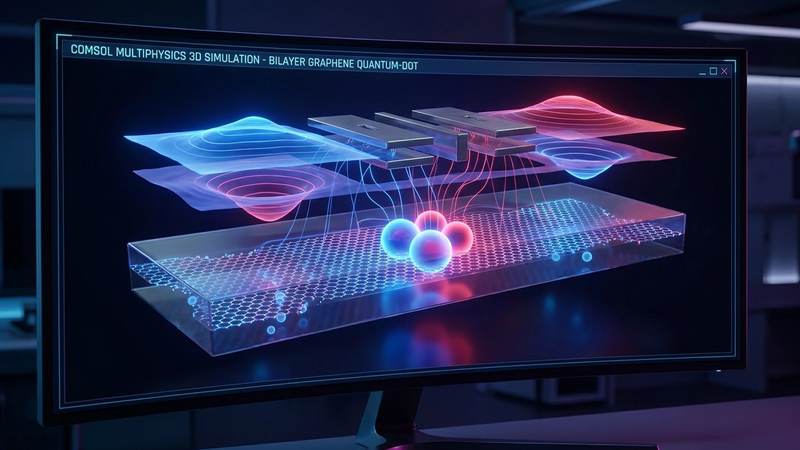
COMSOL Multiphysics is an incredibly powerful finite element analysis software platform that is widely used across various engineering and physics disciplines to simulate coupled physical phenomena. In the context of quantum device engineering, COMSOL is primarily utilized to solve Poisson's equation in three dimensions. Poisson's equation relates the electrostatic potential to the given charge distribution and the spatially varying dielectric permittivity of the materials comprising the device. By inputting the exact three-dimensional computer-aided design geometry of the split gates, plunger gates, dielectric spacer layers, and the graphene channel, researchers can apply specific voltage values to each gate boundary and calculate the resulting electrostatic potential at every point in space.
This computational approach is absolutely crucial because the relationship between the applied gate voltages and the actual potential experienced by an electron in the graphene sheet is highly complex. Fringing fields, cross-capacitance between closely spaced nanoscale gates, and the dielectric screening provided by the hexagonal boron nitride all contribute to a potential landscape that cannot be accurately predicted using simple analytical models. Furthermore, the finite element mesh must be carefully optimized, with an extremely high density of mesh nodes required in the active region of the quantum dot to capture the sharp potential gradients, while a coarser mesh can be used in the bulk dielectric regions to conserve computational resources. The simulations generated by Yoo demonstrate a masterful application of these principles, providing a high-fidelity map of the electric field lines and the resulting potential energy topography that dictates the behavior of the device.
Mapping the Confinement Potential Landscape
The primary objective of applying voltages to the complex gate architecture is to sculpt a specific confinement potential landscape within the bilayer graphene channel. The global back gate and the local top gates are operated in tandem to generate a strong perpendicular displacement field. As previously mentioned, this displacement field breaks the inversion symmetry between the top and bottom layers of the Bernal-stacked graphene, opening a bandgap that can exceed one hundred millielectron volts. Once the bandgap is established, the split gates are biased to push the Fermi level into this newly created forbidden zone, effectively turning the graphene directly beneath them into an insulator. This leaves only a narrow channel of conductive graphene between the split gates.
Subsequently, voltages applied to the plunger gates create localized dips or peaks in the potential energy landscape along this narrow channel. An electron moving through the channel encounters these potential barriers and becomes trapped in the potential well between them. The COMSOL simulations provide a visual and mathematical representation of this process, showing exactly how the depth and width of the confinement potential vary with minute changes in gate voltage. This level of detail is essential for determining the charging energy of the quantum dot, which is the energy required to add one additional electron to the dot, as well as the orbital energy level spacing. Accurate modeling of these parameters allows researchers to tune the device into the few-electron or few-hole regime, which is the operational state required for utilizing the spin or valley degrees of freedom as quantum bits.
Local Electrostatic Offsets and Edge-Dot Activation
While the idealized picture of a single, perfectly defined quantum dot is conceptually straightforward, the reality of nanoscale device fabrication introduces subtle imperfections that can profoundly alter device behavior. One of the most critical insights derived from the COMSOL simulations is the impact of local electrostatic offsets under the split gates. In an ideal scenario, the split gates would generate a perfectly uniform depletion potential. However, minor variations in gate geometry, localized strain in the hexagonal boron nitride, or uneven distribution of the dielectric environment can cause the electrostatic potential to deviate from the ideal design.
The simulations reveal that these local electrostatic offsets can severely modify the primary confinement potential, making it asymmetrical or shallower than intended. More importantly, the computational model demonstrates how these fringing fields and local offsets interact with the physical boundaries of the bilayer graphene channel. The edges of etched graphene devices are known to host localized states due to broken atomic bonds and the accumulation of scattered charge. When the non-uniform electrostatic field generated by the split gates interacts with these physical edges, the potential landscape can dip, creating unintended potential wells. The simulations successfully capture the activation of these additional dot-like regions near the channel edges. Instead of a single, well-isolated quantum dot in the center of the channel, the device inadvertently hosts supplementary parasitic quantum dots at its periphery. This edge-dot activation is a crucial discovery, as it provides a purely electrostatic explanation for anomalous transport signatures that frequently confound experimentalists.
Quantum-Dot-Network Reconstruction
The activation of edge dots transforms the simple, single-dot system into a complex, multi-dot architecture. This phenomenon is described in the research as quantum-dot-network reconstruction. When an edge dot forms in close physical proximity to the intentionally defined central quantum dot, the two regions can interact through both capacitive coupling and quantum mechanical tunnel coupling. Capacitive coupling means that the addition of an electron to the edge dot alters the electrostatic energy required to add an electron to the central dot, and vice versa. Tunnel coupling means that electrons can quantum mechanically tunnel back and forth between the central dot and the edge dot, leading to the hybridization of their molecular orbitals.
The COMSOL electrostatic simulation files provide the foundational data needed to model this network reconstruction. By mapping the exact spatial location and depth of both the primary and the edge-activated dots, researchers can extract the mutual capacitance and estimate the tunnel barriers between them. In experimental transport measurements, such as measuring the current flowing through the device as a function of gate voltages, a single quantum dot produces a highly regular pattern of Coulomb blockade oscillations, often visualized as a series of uniform diamond shapes in a charge stability diagram. However, when a quantum-dot-network undergoes reconstruction due to edge-dot activation, the charge stability diagram becomes significantly more complex, evolving into a honeycomb-like pattern characteristic of double or multiple dot systems. The simulations provide the necessary key to decode these complex experimental transport signatures, proving that they arise not from material defects, but from the intricate electrostatic reality of the device geometry.
Overcoming Challenges in Bilayer Graphene Quantum Computing
The insights gleaned from these electrostatic models are not merely academic; they are highly actionable intelligence for the next generation of quantum hardware engineers. Understanding the mechanisms of edge-dot activation allows researchers to iterate on their device designs to suppress these unwanted parasitic states. For instance, the simulation data suggests that altering the dielectric thickness, modifying the angle and spacing of the split gates, or utilizing different edge-termination techniques during the graphene etching process could significantly reduce the local electrostatic offsets that drive network reconstruction.
As the field of bilayer graphene quantum computing moves towards scaling up the number of qubits, ensuring the uniformity and predictability of each individual quantum dot becomes paramount. Unintended edge dots can act as charge traps, leading to decoherence of the fragile quantum states, or they can cause unwanted crosstalk between neighboring qubits. By utilizing the COMSOL framework established by Ho Yeon Yoo, researchers can pre-screen their gate architectures in a virtual environment, optimizing the electrostatic landscape to guarantee strong confinement and perfect isolation before committing to the expensive and time-consuming process of nanofabrication. This predictive capability is a crucial stepping stone towards realizing the full potential of van der Waals heterostructures in the landscape of solid-state quantum information processing.
FAQ
What is a bilayer graphene quantum dot?
A bilayer graphene quantum dot is a nanoscale region within a two-sheet layer of carbon atoms where charge carriers, such as electrons or holes, are spatially confined in all three dimensions. Unlike single-layer graphene, bilayer graphene can be manipulated with a perpendicular electric field to open a bandgap. By strategically applying voltages to surrounding nanoscale gate electrodes, researchers can create a localized potential well within this bandgap, trapping individual charge carriers to act as artificial atoms for quantum computing applications.
Why is hexagonal boron nitride used in these devices?
Hexagonal boron nitride is utilized as an encapsulation material because it provides an exceptionally clean and atomically flat dielectric environment for the graphene channel. It shares a similar hexagonal crystal lattice structure with graphene but acts as a wide-bandgap insulator. By sandwiching the bilayer graphene between layers of hexagonal boron nitride, the graphene is protected from environmental contaminants, substrate roughness, and trapped charges found in traditional insulators like silicon dioxide, thereby preserving the high mobility and delicate quantum states of the confined electrons.
What is the purpose of COMSOL electrostatic simulations in this research?
COMSOL electrostatic simulations are used to solve complex mathematical equations, specifically Poisson's equation, to model the electric field and potential energy landscape within the quantum device. Because the geometry of the nanoscale gates and the dielectric layers is highly complex, analytical calculations are insufficient. COMSOL allows researchers to input the exact three-dimensional structure and material properties to visualize how applied gate voltages translate into the actual confinement potential experienced by the electrons, helping to optimize device design.
What does edge-dot activation mean in this context?
Edge-dot activation refers to the unintended formation of localized quantum dot-like regions near the physical boundaries of the etched bilayer graphene channel. The simulations reveal that local irregularities or electrostatic offsets generated by the split gates can interact with the physical edges of the graphene. Instead of forming just one central quantum dot, these fringing fields create additional potential wells at the edges, trapping electrons in parasitic dots that complicate the overall behavior of the device.
How does quantum-dot-network reconstruction affect device performance?
Quantum-dot-network reconstruction occurs when the primary central quantum dot interacts with the newly activated edge dots, forming a coupled system. These dots interact via capacitive and tunnel coupling, meaning the charge state of one dot affects the others. This reconstruction drastically alters the electrical transport properties of the device, changing simple, predictable single-dot behaviors into highly complex multi-dot signatures. Understanding this via simulation is critical for interpreting experimental data and designing future devices that avoid unwanted quantum crosstalk.
Conclusion
The comprehensive COMSOL electrostatic modeling of hexagonal boron nitride encapsulated bilayer graphene quantum-dot devices represents a pivotal advancement in the field of nanoelectronics. By meticulously simulating the intricate interplay between complex gate geometries, dielectric environments, and the inherent properties of bilayer graphene, researchers have unveiled the hidden mechanisms governing carrier confinement. The critical discovery of local electrostatic offsets driving edge-dot activation and subsequent quantum-dot-network reconstruction provides a much-needed framework for interpreting complex experimental transport data. As the quantum computing community continues to push the boundaries of solid-state qubit architectures, the foundational computational work demonstrated here will undoubtedly serve as a guiding light. It empowers engineers to design cleaner, more predictable, and highly scalable graphene-based quantum devices, moving us one step closer to realizing the extraordinary promise of next-generation quantum information technologies.
Evaluate Our Quality
Serious about B2B integration? Test our premium Pulsed Electrical Resistive Carbon Heating turbostratic graphene in your lab. 100g sample packs available now.