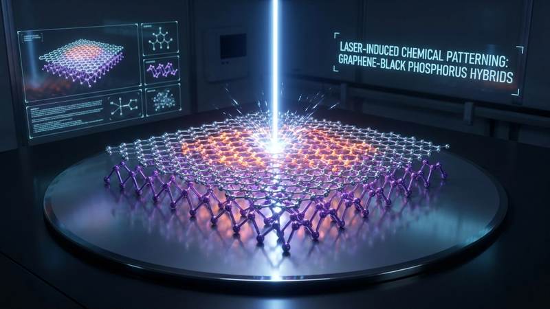
Laser-Induced Chemical Patterning of Graphene-Black Phosphorus Hybrids: A New Era in 2D Materials Engineering
Research conducted by: Jasmin Eisenkolb, Mhamed Assebban, Tobias Dierke, Janina Maultzsch, Andreas Hirsch, Frank Hauke. The dedicated team of researchers behind this groundbreaking study has pushed the boundaries of nanotechnology and materials science. Their collaborative effort merges deep expertise in synthetic chemistry, condensed matter physics, and advanced spectroscopy. By meticulously engineering van der Waals heterostructures, these scientists have provided the scientific community with a novel pathway to manipulate two-dimensional materials at the atomic level, opening doors to next-generation optoelectronics, rewritable circuitry, and quantum devices.
In the rapidly evolving landscape of advanced materials, two-dimensional structures have captured the imagination of physicists and engineers alike. Graphene, the celebrated single layer of carbon atoms arranged in a honeycomb lattice, is renowned for its unparalleled electrical conductivity, mechanical strength, and thermal properties. However, its lack of an inherent bandgap limits its application in traditional digital logic circuits, where the ability to completely shut off an electrical current is paramount. Enter black phosphorus, a fascinating layered material that boasts a highly tunable, direct bandgap and remarkable in-plane anisotropy. While black phosphorus holds immense potential for bridging the gap between zero-bandgap graphene and wide-bandgap transition metal dichalcogenides, it suffers from severe environmental instability. The marriage of these two spectacular materials into a single hybrid system represents a paradigm shift in materials engineering. By stacking them into a van der Waals heterostructure, researchers can theoretically harness the best of both worlds. Yet, integrating and chemically tailoring these extremely delicate atomic layers requires unprecedented precision. This brings us to the core of the recent scientific breakthrough: the highly controlled, laser-induced chemical patterning of graphene and black phosphorus hybrids. This intricate process not only stabilizes the volatile phosphorus but also allows for the customized chemical writing of functional groups, paving the way for bespoke nanoscale devices.
The Promise and Peril of Black Phosphorus
Black phosphorus is arguably one of the most intriguing members of the two-dimensional material family. Unlike its highly reactive and dangerous relative, white phosphorus, black phosphorus is thermodynamically stable in its bulk form. When carefully exfoliated down to a few atomic layers or a single monolayer, commonly referred to as phosphorene, it exhibits a unique puckered honeycomb structure. This specific atomic arrangement gives rise to strong in-plane anisotropy, meaning its electrical, optical, and phonon properties vary significantly depending on the direction in which they are measured. Such characteristics make it an exceptional candidate for directional electronics, polarization-sensitive photodetectors, and advanced thermoelectric devices that require highly specific electron routing. Furthermore, black phosphorus possesses a layer-dependent direct bandgap that spans from the visible to the mid-infrared region of the electromagnetic spectrum. This highly tunable bandgap perfectly complements the zero-bandgap nature of graphene, offering engineers a versatile tool for designing broad-spectrum optoelectronic devices.
Despite these extraordinary attributes, black phosphorus harbors a critical vulnerability that has severely hindered its widespread commercial and technological adoption. The material exhibits an extreme, almost fatal sensitivity to ambient environmental conditions, specifically oxygen and moisture. When exposed to the standard laboratory or atmospheric environment, black phosphorus rapidly degrades, forming oxidized phosphorus species that physically and electronically destroy the carefully exfoliated nanosheets. This degradation process is exponentially accelerated by light exposure, a devastating phenomenon known as photo-oxidation. Consequently, performing standard characterization techniques, such as Raman spectroscopy, on pristine black phosphorus is notoriously difficult and often impossible. The very laser light required to probe the vibrational modes of the crystal lattice imparts enough energy to trigger rapid structural degradation, oxidation, or even complete ablation of the sample. This intense sensitivity creates a massive bottleneck for researchers attempting to study its intrinsic properties or functionalize its surface for specialized applications. Finding a reliable method to stabilize black phosphorus while still allowing for detailed chemical, electrical, and spectroscopic manipulation has thus become a holy grail in the field of two-dimensional materials research.
Engineering the Graphene and Black Phosphorus Heterostructure
To overcome the inherent fragility and environmental instability of pristine black phosphorus, the research team employed an elegant, highly effective solution rooted in the architecture of van der Waals heterostructures. By carefully transferring a layer of chemical vapor deposition grown graphene directly onto the exfoliated black phosphorus nanosheets, they created a robust, intimately coupled hybrid system. In these specialized heterostructures, the individual layers are held together not by strong covalent bonds, but by relatively weak van der Waals forces. This structural arrangement is crucial because it allows each constituent material to largely retain its unique electronic and optical structure while simultaneously benefiting from the physical proximity and complementary properties of the adjacent layer.
In this specific graphene and black phosphorus hybrid architecture, the graphene layer serves a dual, highly synergistic purpose. First and foremost, it acts as an exceptionally effective physical encapsulation layer. Graphene is famously impermeable to standard gases and liquids, including the oxygen and water molecules that spell doom for phosphorene. By blanketing the black phosphorus, the graphene provides a definitive, atom-thick physical barrier against the ambient environment, effectively halting the rapid photo-oxidation and degradation that typically plagues the phosphorus material. Second, the graphene layer provides a robust, chemically versatile canvas for subsequent functionalization. The researchers made a monumental discovery when they observed that the presence of the graphene layer dramatically altered the hybrid system's response to laser irradiation. While the pristine black phosphorus would rapidly deteriorate and burn away under the focused laser beam of a Raman spectrometer, the graphene-capped black phosphorus exhibited remarkable, sustained stability. This protective shielding successfully enabled detailed, long-term Raman spectroscopy investigations that would have been entirely impossible with the bare phosphorus nanosheets. The creation of this heterostructure is a veritable masterclass in nanoscale materials engineering, demonstrating precisely how the strategic combination of two-dimensional materials can neutralize their individual weaknesses while amplifying their collective strengths for advanced technological applications.
Laser-Induced Covalent Functionalization
With the highly reactive black phosphorus safely encapsulated and stabilized by the protective graphene overlayer, the researchers advanced to the most critical and innovative phase of their study: spatially resolved chemical patterning. The functionalization of two-dimensional materials is an absolutely essential step for tailoring their electronic, optical, and chemical properties for specific device applications, such as biological sensors or logic gates. In this comprehensive study, the team focused their efforts on covalent functionalization, a complex process that involves forming strong, permanent chemical bonds between the basal plane of the material and external molecules. To achieve this sophisticated chemical tailoring, they utilized specially formulated dibenzoyl peroxide-based precursors.
The true innovation within this research lies in the specific method used to trigger the chemical reaction. Rather than relying on traditional bulk heating or harsh wet-chemical processes that could potentially damage the delicate underlying heterostructure or offer absolutely no spatial control over the reaction, the team employed highly focused laser irradiation. The dibenzoyl peroxide precursors are intricately designed to decompose upon exposure to specific, targeted laser wavelengths, a process that generates highly reactive phenyl radicals. These newly formed radicals then immediately attack the sp2-hybridized carbon lattice of the top graphene layer, covalently attaching themselves and locally disrupting the conjugated pi-electron system. Because the chemical reaction is driven entirely by the localized thermal and photonic energy of the tightly focused laser beam, the researchers achieved unprecedented spatially resolved functionalization. This remarkable capability means they could essentially write complex chemical patterns and microscopic circuits directly onto the surface of the heterostructure with sub-micron precision, functioning much like a microscopic, light-driven pen.
Crucially, this precise laser-induced chemical patterning was achieved under exceptionally mild laser conditions. Because the top graphene layer efficiently absorbs the incident laser energy and facilitates the radical generation process, the underlying, highly sensitive black phosphorus remains largely undisturbed by the violent chemical process occurring just nanometers above it. The meticulous control over the laser power, wavelength, and exposure time ensured that the covalent functionalization was confined exclusively to the top graphene layer, leaving the highly valuable electronic properties and the delicate crystal lattice of the black phosphorus substrate completely intact. This advanced methodology represents a massive leap forward in the fabrication of complex, chemically patterned two-dimensional devices, offering a scalable route toward customized nanoscale engineering.
Interference Effects and Thickness-Dependent Raman Modulation
As the researchers diligently probed the newly synthesized and chemically patterned heterostructures using advanced Raman spectroscopy, they encountered a fascinating, highly complex optical phenomenon that required deep analytical modeling. Raman spectroscopy is a powerful, non-destructive analytical technique that relies on the inelastic scattering of monochromatic light to provide incredibly detailed information about molecular vibrations, crystal structure, and chemical bonding within a material. In the realm of two-dimensional materials, it is universally recognized as the gold standard for determining layer thickness, identifying structural strain, and measuring chemical doping levels. However, in the specific case of the graphene and black phosphorus hybrids, the Raman signal generated by the top graphene layer exhibited highly unusual, highly pronounced thickness-dependent intensity modulations.
Specifically, the researchers observed that the intensity of the characteristic graphene Raman bands, such as the primary G band and the secondary 2D band, varied dramatically and predictably depending on the exact nanometer thickness of the underlying black phosphorus flake. In certain localized regions, the graphene signal was enormously amplified, while in other adjacent regions, it was almost entirely suppressed or silenced. The research team correctly and astutely identified this perplexing behavior as the direct result of multiple optical interference effects occurring within the stratified, multi-layered heterostructure. When the incident laser light strikes the sample, it does not simply reflect off the top surface; instead, it undergoes a complex, cascading series of reflections and refractions at the various interfaces between the ambient air, the graphene layer, the black phosphorus flake, and the underlying silicon dioxide substrate. The inelastically scattered Raman light generated within the graphene layer undergoes similar, highly complex multiple reflections before finally exiting the sample and reaching the spectrometer's detector.
Depending on the precise optical path length of these traveling light waves, which is directly and mathematically dictated by the physical thickness of the black phosphorus layer, these multiple reflected waves can interfere with each other either constructively or destructively. Constructive interference leads to a massive, easily measurable enhancement of the Raman signal, whereas destructive interference causes severe signal suppression. The researchers did not merely observe this optical phenomenon; they meticulously quantified and modeled it using classical optics principles and the advanced transfer matrix method. By accurately calculating the interference-induced enhancement factors across a range of thicknesses, they successfully transformed a potentially confusing optical artifact into a highly powerful analytical tool. This comprehensive optical mathematical model allowed them to precisely determine the exact thickness of the black phosphorus flakes simply by analyzing the intensity modulation of the overlying graphene Raman bands, providing a rapid, non-invasive, and highly accurate method for heterostructure characterization.
Reversibility Through Temperature-Dependent Raman Spectroscopy
The ability to precisely attach chemical functional groups to a two-dimensional material is an undeniably powerful tool, but the subsequent capacity to remove those groups and entirely restore the material to its pristine, unadulterated state elevates the technology to an entirely new paradigm of utility. Chemical reversibility is a highly sought-after characteristic in modern materials science, as it directly paves the way for the development of rewritable electronic circuits, reusable environmental sensors, and highly adaptive optoelectronic devices that can change their function on demand. To thoroughly investigate the stability and the ultimate reversibility of the laser-induced covalent functionalization, the research team conducted exhaustive, highly controlled temperature-dependent Raman spectroscopy studies.
By carefully placing the functionalized graphene and black phosphorus heterostructures into a specialized, atmosphere-controlled heating stage, the researchers gradually and systematically elevated the ambient temperature while continuously monitoring the real-time Raman spectra. The covalently attached phenyl groups clearly manifest themselves in the Raman spectrum of the graphene layer through the sudden emergence of a distinct, highly measurable defect-induced mode, universally known as the D band. The mathematical intensity of this D band, particularly when calculated relative to the primary G band, serves as a direct, highly reliable quantitative measure of the overall degree of chemical functionalization. As the temperature within the heating stage was incrementally increased, the researchers observed a clear, continuous, and systematic decrease in the intensity of the D band.
This real-time spectral evolution provided unambiguous, undeniable evidence that the applied thermal energy was effectively breaking the strong covalent bonds between the attached phenyl groups and the underlying graphene lattice, causing the functional molecules to physically detach and desorb from the surface of the material. Upon reaching a specific, critical threshold temperature, the D band completely vanished from the recorded Raman spectrum, and the characteristic, highly recognizable signature of pristine, defect-free graphene was fully and entirely restored. This meticulously documented temperature-dependent defunctionalization definitively confirms that the laser-induced chemical patterning is not only a highly controllable process but also an entirely reversible one. The technological implications of this demonstrated reversibility are profound and far-reaching. It strongly suggests that complex chemical circuits and logic gates could be optically written into the heterostructure, utilized for a specific computational or sensing task, and then thermally erased at a later time, returning the nanoscopic device to a blank slate ready for an entirely new configuration or purpose.
Frequently Asked Questions
Question: What exactly are two-dimensional materials and why are they considered so important to modern science?
Answer: Two-dimensional materials are extremely thin crystalline substances consisting of merely a single layer of atoms. Graphene, a single layer of carbon atoms arranged in a hexagonal lattice, is the most famous and widely studied example, known globally for its incredibly high electrical conductivity and physical strength. These materials are critically important because their ultra-thin, planar nature restricts electron movement to two dimensions, which gives them unique quantum mechanical properties that differ vastly from their standard three-dimensional bulk counterparts. They are widely considered the foundational building blocks for the next generation of ultra-fast, highly flexible, and highly efficient electronic and optoelectronic devices.
Question: Why did the researchers specifically choose to combine graphene with black phosphorus for this study?
Answer: Graphene has excellent electrical conductivity but completely lacks a natural bandgap, making it incredibly difficult to turn off electrical currents in digital logic applications, which is necessary for computer processors. Black phosphorus, on the other hand, has a highly tunable direct bandgap and excellent charge carrier mobility, but it degrades rapidly and violently when exposed to air or under laser light. By combining them into a van der Waals heterostructure, the researchers ingeniously used the graphene layer to physically encapsulate and protect the fragile black phosphorus from the environment, while successfully maintaining the highly beneficial electronic properties of both materials.
Question: How does the laser-induced chemical patterning process actually work at the molecular level?
Answer: The researchers first coated the surface of the heterostructure with a specific dibenzoyl peroxide-based chemical precursor. When they directed a highly focused laser beam onto the surface, the intense light energy caused the precursor molecules to break down into highly reactive chemical radicals. These newly formed radicals then immediately formed strong covalent chemical bonds specifically with the carbon atoms in the top graphene layer. By carefully moving the laser beam across the sample, the researchers could precisely draw complex chemical patterns onto the material at the microscopic level without damaging the delicate underlying black phosphorus.
Question: What is optical interference and how did it impact the findings of this specific study?
Answer: Optical interference is a physical phenomenon that occurs when light waves bounce off different layers of a thin material and either combine to become stronger or cancel each other out, depending on their alignment. In this study, the laser light bounced continuously between the top graphene, the middle black phosphorus, and the bottom substrate. Depending on the exact nanometer thickness of the black phosphorus layer, this bouncing caused the Raman spectroscopy signal of the graphene to become much brighter or much dimmer. The researchers created a complex mathematical model of this effect, allowing them to brilliantly use the brightness of the graphene signal to accurately measure the hidden thickness of the black phosphorus layer.
Question: Is the chemical functionalization created by the laser permanent, or can it be removed?
Answer: The comprehensive study demonstrated that the chemical patterning is entirely reversible through the careful application of heat. The researchers performed temperature-dependent Raman spectroscopy, gradually heating the functionalized heterostructure in a controlled environment. As the temperature steadily rose, the added thermal energy broke the covalent bonds holding the chemical groups to the graphene lattice. Eventually, the functional groups detached completely as a gas, and the material returned entirely to its original, pristine state. This proven reversibility is highly valuable for creating rewritable electronic components and highly reusable environmental sensors.
Conclusion
In summary, the intricate, highly controlled laser-induced chemical patterning of graphene and black phosphorus van der Waals heterostructures represents a truly monumental leap forward in the complex realm of nanoscale materials engineering. By successfully harnessing the robust protective qualities of graphene to stabilize the notoriously fragile and reactive black phosphorus, the dedicated research team has unlocked a versatile, highly stable new platform for advanced materials science and device fabrication. The demonstrated ability to spatially resolve covalent functionalization using surprisingly mild laser conditions, seamlessly coupled with the profound, mathematically modeled understanding of thickness-dependent optical interference effects, provides engineers with unprecedented, highly precise control over the architecture of two-dimensional devices.
Furthermore, the clearly demonstrated thermal reversibility of these sophisticated chemical modifications strongly hints at a rapidly approaching future populated by dynamic, rewritable nanoscale circuitry and highly adaptive, reusable chemical sensors. As the global technological demand for smaller, faster, and exponentially more energy-efficient technologies continues to accelerate at a breakneck pace, the foundational scientific insights provided by this meticulous study will undoubtedly catalyze the development of next-generation optoelectronics, advanced quantum computing architectures, and sophisticated chemical sensing platforms. This groundbreaking research not only solves a critical, long-standing stability issue that has historically plagued black phosphorus adoption but also firmly establishes a highly robust, easily scalable methodology for the bespoke chemical tailoring of complex hybrid nanomaterials.
Evaluate Our Quality
Serious about B2B integration? Test our premium Pulsed Electrical Resistive Carbon Heating turbostratic graphene in your lab. 100g sample packs available now.