Direct Writing Graphene: Advances in Nanopatterning
The Evolution of Graphene Fabrication

Figure 1. Graphene fabrication methods timeline showing bulk fabrication (exfoliation), film growth (CVD, PVD), and direct writing techniques (laser, electron beam). Adapted from Abrahamczyk et al., Advanced Materials 2025.
A comprehensive review published in Advanced Materials in 2025 by researchers Szymon Abrahamczyk, Ondřej Sakreida, Alicja Bachmatiuk, Gražyna Simha Martynková, and Mark H. Rümmeli critically examines modern graphene synthesis. Since its initial isolation via mechanical exfoliation, the scientific community has relentlessly pursued scalable manufacturing processes capable of preserving its remarkable physical properties. Single-layer pristine graphene operates as a zero-bandgap material allowing the conduction of massless Dirac fermions, translating to exceptional electrical conductivity. Maintaining this high conductivity at the nanoscale requires fabrication methods that avoid introducing structural defects or chemical impurities into the delicate carbon lattice. Early approaches relied heavily on breaking down bulk graphite through mechanical, chemical, or liquid-phase exfoliation strategies. While these bulk techniques successfully introduced graphene to commercial applications, they consistently suffer from poor control over domain size and defect density.
To address the limitations of bulk exfoliation, the industry increasingly turned toward advanced bottom-up growth methodologies. Chemical vapor deposition emerged as a dominant technique, utilizing gaseous carbon sources that disintegrate on catalytic metallic surfaces like copper. This high-temperature process allows for substantial control over layer count, enabling the production of continuous monolayer graphene films across large areas. Copper substrates prove particularly advantageous for single-layer growth due to low carbon solubility, whereas nickel substrates often yield multiple layers during cooling. Despite producing high-quality material, chemical vapor deposition requires extreme processing temperatures and specialized substrates that limit immediate device integration. Transferring these delicate films from catalytic metals to insulating substrates introduces mechanical stress, frequently resulting in wrinkles and degraded electronic performance.
Epitaxial growth on silicon carbide offers another high-quality alternative for producing wafer-scale arrays with excellent intrinsic crystallinity. This technique sublimates silicon atoms from the substrate surface at ultra-high temperatures, leaving behind a highly ordered carbon lattice. The resulting epitaxial material exhibits minimal defects and perfectly aligns with existing conventional semiconductor manufacturing infrastructures. The prohibitively high cost of silicon carbide wafers and the extreme thermal budget heavily restrict the widespread scalability of this specific approach. Pyrolysis of carbon-rich polymer precursors provides a more versatile, transfer-free route toward direct material formation on various arbitrary target substrates. While pyrolysis greatly simplifies process integration, it typically yields a higher degree of structural disorder compared to advanced epitaxial methods.
Characterizing Graphene Quality

Figure 2. SEM images and Raman spectra comparing graphene grown via epitaxial growth on SiC (A) and monolayer graphene grown by CVD transferred onto Si (B). The characteristic G, D, and 2D bands provide quality assessment metrics. Adapted from Abrahamczyk et al., Advanced Materials 2025.
The intrinsic quality of synthesised graphene dictates its ultimate utility in advanced nanoelectronics, making precise characterization absolutely essential. Researchers primarily evaluate quality based on stacked layers, structural anomalies, chemical uniformity, and the physical size of individual continuous domains. Pristine single-layer graphene features conduction and valence bands touching at a single Dirac point, facilitating unhindered charge carrier transport. Introducing a second layer immediately generates interlayer interactions and spin-orbit coupling, effectively creating a finite bandgap and increasing effective carrier mass. Structural deviations are classified into point defects like vacancies, line defects such as grain boundaries, and plane defects including localized folds. These inevitable distortions alter the local electronic environment, introducing beneficial tunable bandgaps while simultaneously scattering charge carriers and reducing overall mobility.
Chemical doping serves as a primary mechanism for intentionally modifying the electronic structure of the pure carbon lattice. Incorporating heteroatoms such as boron, nitrogen, phosphorus, or oxygen directly into the hexagonal framework allows the material to accept or donate electrons. Surface functionalization, particularly through intensive oxidation, disrupts the pure sp2 hybridization and introduces localized sp3 hybridized regions that act as insulators. The deliberate adsorption of metallic atoms or specialized molecules onto the surface can also induce charge transfer without physically breaking carbon bonds. Beyond chemical modifications, the physical dimensions of the crystalline domains play a massive role in dictating macroscopic electrical performance. Small domains below ten nanometers experience severe quantum confinement effects, whereas large monocrystalline sheets preserve the inherent ballistic transport characteristics.
Raman spectroscopy remains the universally accepted, non-destructive gold standard for quantifying these distinct quality metrics in carbon nanomaterials. The technique relies on measuring specific vibrational modes of the carbon lattice, primarily focusing on the prominent G, D, and 2D bands. The G band, appearing near fifteen hundred and eighty inverse centimeters, originates from the continuous stretching of bonds within the perfect hexagonal lattice. The D band emerges around thirteen hundred and fifty inverse centimeters and corresponds to the breathing motion of six-membered carbon rings. Because this specific breathing mode requires a break in symmetry to conserve momentum, the D band intensity directly quantifies local defect density. Analyzing the full width at half-maximum and relative intensity ratios of these distinct bands allows researchers to definitively determine structural sp2 purity.
Conventional Lithography vs. Direct Writing

Figure 3. Comparison of conventional top-down lithographic patterning methods versus emerging direct-write approaches for graphene nanofabrication, highlighting the key advantages and limitations of each paradigm. Adapted from Abrahamczyk et al., Advanced Materials 2025.
Integrating high-quality graphene into commercial electronic devices heavily relies on complex patterning techniques adapted from the established silicon semiconductor industry. Conventional top-down lithographic approaches require depositing a protective photoresist layer, exposing specific regions to ultraviolet light, and chemically etching away unprotected material. Applying these aggressive chemical and physical processing steps to atomically thin carbon layers introduces severe complications that degrade ultimate device performance. Residual photoresist molecules frequently bind tightly to the highly reactive surface, acting as persistent chemical contaminants that alter localized charge carrier concentrations. The etching plasmas utilized to define the geometric patterns physically bombard the exposed lattice edges, creating jagged boundaries loaded with reactive dangling bonds. These chemically unstable edges relentlessly scatter passing electrons and significantly elevate the overall electrical resistance of the resulting patterned nanostructures.
The fundamental requirement of transferring chemical vapor deposition graphene from its native catalytic growth substrate to a target wafer exacerbates these challenges. Transfer protocols typically involve intermediate polymer support films that must be subsequently dissolved using harsh, environmentally damaging organic solvents. This manual transfer process inevitably traps microscopic water droplets, atmospheric gases, and stubborn polymer residues completely beneath the destination substrate. Achieving precise alignment of pre-grown graphene sheets across multi-layered heterogeneous device architectures routinely pushes the operational limits of current optical hardware. The mechanical strain induced during the transfer phase regularly produces microscopic tears and overlapping folds that ruin continuous electrical pathways. Consequently, the yield and reliability of devices fabricated through these traditional transfer and etch pathways remain insufficient for demanding industrial scale manufacturing.
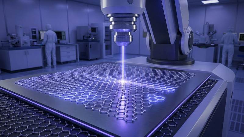
Direct-write technologies represent a radical departure from these highly problematic top-down patterning and manual transfer methodologies. These advanced approaches utilize focused beams of energy or particles to induce localized sp2 carbon formation exactly where required on the final substrate. By eliminating the need for sacrificial photoresists, chemical etchants, and hazardous physical transfer steps, direct writing successfully minimizes external contamination. This bottom-up strategy enables the precise fabrication of intricate nanoscale geometries on fragile or unconventional substrates that cannot survive traditional lithography. Engineers can dynamically adjust the design patterns in real-time through precise software control, bypassing the costly physical mask fabrication phase entirely. The transition toward maskless, transfer-free patterning clearly holds the key to unlocking scalable manufacturing for next-generation carbon-based optoelectronics and quantum devices.
Focused Electron Beam Induced Deposition

Figure 4. Focused Electron Beam Induced Deposition (FEBID) process for direct graphene writing. The electron beam dissociates precursor molecules on the substrate surface, enabling bottom-up carbon nanostructure fabrication. Adapted from Abrahamczyk et al., Advanced Materials 2025.
Focused electron beam induced deposition stands out as a premier direct-write technique capable of achieving extraordinary spatial resolution. The process operates within a high-vacuum scanning electron microscope chamber equipped with a specialized gas injection system. Gaseous precursor molecules are continuously injected near the target substrate, where they temporarily adsorb onto the solid surface via weak physical interactions. A highly focused primary electron beam rapidly scans across the substrate surface according to a predefined, precisely calibrated digital pattern. The interaction between the primary beam and the substrate generates a localized cascade of low-energy secondary electrons that trigger chemical dissociation. The volatile byproducts of this dissociation reaction are pumped away by the vacuum system, leaving behind a permanently deposited solid carbon nanostructure.
The specific precursor chemistry utilized during the deposition process fundamentally dictates the structural quality and elemental purity of the resulting traces. Ideal precursors for graphene synthesis must possess a high carbon-to-hydrogen ratio and exhibit highly favorable dissociation kinetics under electron irradiation. Aromatic compounds containing pre-formed hexagonal carbon rings often serve as excellent starting materials due to their structural similarity to the graphene lattice. When the secondary electrons selectively cleave the peripheral bonds of these aromatic precursors, the remaining carbon fragments naturally cross-link into extended networks. If the dissociation process remains incomplete, significant quantities of sp3 hybridized amorphous carbon and residual hydrogen atoms become permanently trapped within the structure. Researchers continuously optimize custom precursor molecules designed specifically to dramatically lower the activation energy required for complete graphitisation during electron beam exposure.
Precise manipulation of specific beam parameters provides operators with extensive control over the final geometry and electrical properties of the deposited material. The acceleration voltage of the primary beam determines the penetration depth and the lateral spread of the secondary electron emission volume. Higher acceleration voltages generally confine the primary beam to a smaller spot size, theoretically improving the ultimate nanoscale patterning resolution limits. The total beam current dictates the localized electron dose rate, which must be carefully balanced against the continuous replenishment rate of the gas. If the electron dose excessively outpaces the precursor arrival rate, the deposition process becomes severely supply-limited, resulting in uneven structural voids. The specific dwell time at each individual pixel location influences the local heating effect, thermally assisting the localized structural ordering of carbon atoms.
Polymer-to-Graphene Conversion

Figure 5. Polymer-to-Graphene (P2G) conversion process showing how focused electron or laser beams transform polymer precursors directly into graphene nanostructures on various substrates. Adapted from Abrahamczyk et al., Advanced Materials 2025.
Polymer-to-graphene conversion offers a versatile approach for fabricating conductive carbon traces directly on insulating substrates without requiring complex vacuum chambers. The process begins by depositing a uniform thin film of a carbon-rich polymer, typically polymethyl methacrylate, onto the desired target surface. This polymeric precursor film is subsequently exposed to tightly focused thermal or radiation energy sources that initiate localized chemical decomposition. As the irradiated regions heat up dramatically, the polymer chains undergo rapid pyrolysis, driving off oxygen and hydrogen atoms as volatile gases. The remaining pure carbon atoms dynamically rearrange themselves to minimize surface energy, ultimately crystallizing into a continuous hexagonal sp2 bonded network. The surrounding unexposed polymer remains completely intact, acting as a natural protective matrix or allowing for simple chemical removal post-processing.
The thermodynamic efficiency of this structural transformation heavily depends on the presence of appropriate catalytic interfaces during the localized conversion process. Depositing ultra-thin layers of transition metals like copper, nickel, or chromium directly beneath the polymer film significantly lowers the required graphitisation temperature. These catalytic metallic layers actively assist in rapidly breaking the strong carbon-carbon single bonds within the amorphous polymer backbone. The liberated carbon atoms temporarily dissolve into the metallic matrix before precipitating back to the surface as highly ordered crystalline graphene upon cooling. Implementing carefully controlled mixtures of hydrogen and argon gases during the thermal treatment helps chemically etch away structural defects and prevents unwanted oxidation. Following the complete structural conversion, the sacrificial metallic catalysts can be selectively dissolved using mild wet etchants leaving the graphene anchored.
This specific conversion methodology delivers massive advantages for the seamless integration of carbon nanomaterials into complex three-dimensional device architectures. The extreme spatial confinement of the localized energy source dictates the final structural resolution limits, completely eliminating the necessity for subsequent reactive etching. Engineers can easily spin-coat the liquid polymer precursor over highly irregular topographies, enabling the direct writing of conductive interconnects across microscopic trenches. Modulating the applied energy density allows for precise control over the final structural thickness, ranging from isolated monolayers to conductive graphitic stacks. The technique also supports the simultaneous creation of localized doped regions by intentionally blending specific heteroatom-containing molecular additives directly into the initial solution. As industrial manufacturing increasingly demands flexible and transparent electronics, this robust transfer-free patterning capability positions polymer conversion as a highly scalable commercial pathway.
Laser-Assisted Graphitisation

Figure 6. Laser-assisted graphitisation demonstrating direct-write capability for graphene patterning. The technique enables rapid, maskless fabrication of conductive graphene traces on polymer and carbon-rich substrates. Adapted from Abrahamczyk et al., Advanced Materials 2025.
Laser-assisted graphitisation leverages tightly focused beams of intense light to drive the localized transformation of insulating precursors into conductive carbon pathways. The technique typically employs either continuous-wave or pulsed laser systems operating across various wavelengths from the ultraviolet to the infrared spectrum. When the laser beam irradiates a suitable precursor, such as a polyimide film or graphene oxide, it rapidly induces localized heating. This precise photothermal mechanism instantly elevates the microscopic focal volume to temperatures exceeding two thousand degrees Celsius within mere milliseconds. The extreme thermal shock forcefully breaks the complex molecular bonds of the precursor material, violently expelling non-carbon heteroatoms as gaseous effluents. The residual carbon atoms rapidly condense and undergo sp2 carbon formation, creating durable graphitic traces directly along the programmed scanning path.
Achieving high-quality crystalline traces requires meticulous optimization of several interconnected laser processing parameters to prevent uncontrolled thermal damage. The total optical power delivered to the substrate must precisely match the specific thermal degradation threshold of the chosen precursor material. The scanning speed of the laser beam dictates the exact duration of the thermal exposure, directly influencing the final degree of carbon lattice ordering. If the beam moves too slowly, excessive heat accumulation causes severe ablation, physically vaporizing the newly formed carbon and creating deep structural trenches. The physical size of the focused optical spot fundamentally determines the ultimate resolution limits, typically restricting features to the micrometer scale due to optical diffraction. Employing specialized optics and utilizing shorter wavelength ultraviolet lasers can successfully compress the focal spot size closer to the sub-micrometer dimensional regime.
The remarkable speed and complete scalability of laser writing make it exceptionally attractive for the rapid prototyping of flexible electronic components. Manufacturers can utilize standard industrial roll-to-roll processing equipment to continuously feed inexpensive polymer sheets directly under stationary programmable optical scanning heads. This high-throughput capability facilitates the mass production of flexible electrochemical supercapacitors, wearable biometric sensors, and transparent radio frequency antennas. By carefully modulating the optical intensity during the writing process, engineers can generate unique three-dimensional porous carbon morphologies that dramatically increase active surface areas. The localized nature of the thermal interaction prevents the bulk substrate from experiencing temperature spikes, ensuring compatibility with thermally sensitive plastic foils. As advanced beam steering technologies continue to improve, laser-assisted graphitisation stands ready to dominate the commercial production of carbon-based diagnostic devices.
Focused Ion Beam Modification
Focused ion beam technology provides an precise alternative particle-based approach for the direct manipulation and nanoscale patterning of carbon materials. Instead of utilizing lightweight electrons, this advanced technique accelerates heavy, positively charged ions, typically gallium or helium, toward the target surface. The substantial mass of these energetic ions allows them to transfer significant kinetic energy directly to the atoms within the substrate lattice. Operating at extremely low beam currents, focused ion systems can locally dissociate injected carbonaceous precursor gases to build specialized carbon nanostructures atom by atom. When utilizing lighter helium ions, the localized interaction volume remains exceptionally narrow, enabling spatial resolution limits down to the sub-ten nanometer scale. This extreme precision allows researchers to carve intricate quantum dots or ultra-narrow nanoribbons into synthesized graphene sheets without relying on protective masks.
The underlying mechanism of these heavy particle interactions relies on complex collision cascades generated deep within the target material. As the accelerated primary ion forcefully strikes the solid surface, it physically knocks native carbon atoms out of their established hexagonal lattice positions. This controlled sputtering effect enables the ultra-precise direct milling of microscopic geometries, physically cutting away unwanted material to define specific electrical pathways. By intentionally lowering the applied acceleration voltage, operators can transition from destructive physical milling to constructive localized lattice defect engineering. Carefully controlled ion bombardment introduces specific densities of point vacancies and line defects that systematically alter the local electronic bandgap of the targeted region. These precisely engineered localized defect states serve as crucial active sites for subsequent chemical functionalization or for tuning the catalytic properties of the modified surface.
Despite its unmatched precision, focused ion beam processing introduces several unique structural challenges that require careful mitigation strategies. The massive kinetic energy of the incoming particles frequently amorphizes the surrounding crystalline lattice, converting conductive sp2 carbon into insulating sp3 hybridized domains. Heavy gallium ions inevitably become permanently implanted within the substrate, acting as metallic impurities that severely scatter passing charge carriers. Utilizing lighter noble gas ions like helium or neon significantly reduces this chemical contamination risk while simultaneously minimizing collateral damage to the pristine lattice. High-temperature post-annealing treatments executed under ultra-high vacuum conditions are frequently necessary to heal localized structural damage and restore the original hexagonal carbon symmetry. Balancing the destructive nature of physical ion sputtering with the need for high-quality crystalline retention remains the primary operational hurdle for this methodology.
The Road Ahead: Challenges and Future Directions
While direct-write technologies present a compelling alternative to traditional lithography, widespread industrial adoption remains hindered by several persistent technical limitations. The most significant challenge involves the frequent occurrence of only partial graphitisation during the localized energy exposure phase. Current localized heating and electron-induced dissociation methods often leave behind unacceptable levels of amorphous carbon and unreacted precursor fragments within the deposited traces. These microscopic structural impurities drastically reduce the overall charge carrier mobility and elevate the electrical resistance far beyond the theoretical limits of pristine graphene. Achieving true nanoscale resolution fidelity also requires overcoming complex hardware constraints related to thermal diffusion and secondary particle scattering within the substrate matrix. Until engineers can reliably produce purely crystalline, defect-free sp2 carbon structures at high writing speeds, these techniques will struggle to replace silicon manufacturing lines.
Overcoming these substantial material quality issues requires the development of sophisticated in situ processing capabilities under controlled environments. Future direct-write systems must seamlessly integrate advanced heating stages and reactive gas delivery networks directly into the fabrication chambers. Implementing real-time localized optical spectroscopy allows automated software systems to dynamically monitor the precise degree of graphitisation during the writing process. Combining these advanced beam control systems with novel graphitizable precursors designed with low activation barriers will significantly enhance the final crystalline purity. Exploring atomically thin catalytic capping layers that locally confine the applied thermal energy could prevent unwanted heat diffusion and sharpen the ultimate patterning resolution. The continuous refinement of sophisticated computational algorithms will help optimize the intricate interplay between beam scanning speeds, precursor flow rates, and localized thermal management.
The successful resolution of these specific hardware and chemical challenges will unlock the potential of direct-write nanomanufacturing. Transitioning these precise bottom-up techniques from isolated laboratory curiosities to fully automated, wafer-scale production environments demands coordinated interdisciplinary collaboration across materials science and mechanical engineering. Scalable, high-fidelity graphene components will directly enable the commercialization of ultra-fast flexible microprocessors, efficient energy storage architectures, and advanced biomedical diagnostic implants. Eliminating the chemical waste streams associated with traditional photoresists and hazardous wet etchants also aligns perfectly with modern global initiatives promoting sustainable green semiconductor manufacturing. As localized beam generation technologies become increasingly affordable and reliable, decentralized maskless fabrication facilities could dramatically disrupt traditional global semiconductor supply chains. Ultimately, the relentless pursuit of perfect direct carbon writing ensures that this remarkable two-dimensional material will eventually fulfill its promise to redefine solid-state electronics.
Frequently Asked Questions
What makes direct writing superior to traditional lithography for patterning sensitive nanomaterials? Traditional lithography requires multiple masking and chemical etching steps that inevitably introduce severe surface contaminants. Direct writing completely eliminates these destructive intermediary steps by utilizing focused energy beams. This elegant bottom-up approach preserves the delicate hexagonal carbon lattice while drastically reducing processing time. Engineers can seamlessly pattern highly complex architectures directly onto fragile substrates that cannot survive standard processing.
How does Raman spectroscopy accurately determine the structural quality of newly patterned graphene traces? Raman spectroscopy precisely measures unique vibrational phonon modes to non-destructively assess crystalline integrity and defect density. The specific intensity ratio between the defect-activated D band and the primary graphitic G band provides a reliable quantitative metric. Analyzing the exact shape and spectral positioning of the resonant 2D band further confirms the specific number of stacked layers. This rapid optical characterization allows researchers to continuously calibrate their direct-write beam parameters to maximize sp2 purity.
What precise role does precursor chemistry play during focused electron beam induced deposition? The molecular structure of the chosen precursor gas fundamentally dictates the final elemental composition of the deposited nanostructure. Carbon-rich aromatic precursors featuring low dissociation barriers naturally yield much higher purity crystalline networks under secondary electron irradiation. Carefully optimizing these distinct chemical properties systematically minimizes the unwanted codeposition of insulating amorphous carbon. Selecting the ideal precursor ultimately enhances the macroscopic electrical conductivity of the written patterns for advanced device integration.
Why is achieving pure sp2 carbon formation so difficult when utilizing localized heating techniques? Localized beam heating inherently creates incredibly steep temperature gradients that severely disrupt the uniform reorganization of free carbon atoms. The resulting rapid microscopic cooling rates frequently trap structural defects and leave significant amounts of amorphous material. Achieving a flawless hexagonal lattice requires perfectly balanced thermal energy delivery to ensure the complete expulsion of non-carbon heteroatoms. Extensive empirical parameter optimization and the strategic integration of catalytic metallic substrates remain essential to maximize the crystalline fraction.
What define the primary spatial resolution limits of current direct-write graphene technologies? The ultimate patterning resolution is largely constrained by the physical interaction volume of the primary energy beam. While advanced electron beams can be easily focused to sub-nanometer spot sizes, the unpredictable scattering of secondary electrons broadens the deposition area. Optical techniques face fundamental physical diffraction limits that heavily restrict focused laser spots to the micrometer regime. Overcoming these strict fundamental limits requires new generations of advanced beam control hardware combined with highly localized precursor dissociation mechanisms.
Conclusion
The relentless pursuit of advanced nanoscale manufacturing has driven a vital transition from destructive top-down lithography to highly precise bottom-up direct writing. Exhaustive research documented in recent comprehensive academic reviews clearly demonstrates the severe limitations of relying on sacrificial resists and hazardous chemical etchants. By eliminating physical transfer steps and complex masking requirements, these emerging direct-write technologies protect the fragile electronic properties of atomically thin carbon networks. Techniques such as focused electron beam induced deposition and laser-assisted graphitisation offer unprecedented spatial control over localized carbon lattice formation. These innovative approaches empower engineers to seamlessly integrate conductive nanomaterials directly into complex three-dimensional device architectures without compromising structural integrity. The ability to dynamically alter design geometries through purely digital software control drastically accelerates the rapid prototyping phase for novel optoelectronic components.
Fully realizing the commercial promise of these maskless techniques requires a deep fundamental mastery of the underlying physicochemical transformation mechanisms. Researchers must rigorously investigate the complex thermodynamics governing localized sp2 carbon formation under extreme thermal and electronic stimulation. The strategic development of highly specialized precursor molecules designed specifically for rapid dissociation will significantly minimize the codeposition of insulating amorphous carbon. Implementing sophisticated real-time beam modulation hardware will help precisely manage the severe microscopic temperature gradients that currently restrict spatial resolution limits. Utilizing advanced non-destructive metrology tools like Raman spectroscopy ensures that the engineered crystalline quality meets the exacting standards required by the modern semiconductor industry. Collaborative efforts bridging computational modeling and experimental materials science remain absolutely critical for optimizing these highly sensitive localized reaction environments.
The successful maturation of direct-write graphene fabrication holds massive implications for the future landscape of global semiconductor manufacturing and sustainable electronics. Moving these precise methodologies beyond controlled laboratory settings into high-throughput industrial fabrication facilities represents the next great hurdle for materials engineers. As the necessary vacuum hardware and advanced beam steering optics become increasingly accessible, decentralized maskless production lines will rapidly proliferate. This technological shift will directly accelerate the widespread commercialization of advanced quantum sensors, flexible transparent microprocessors, and ultra-dense energy storage devices. The strategic elimination of toxic chemical waste streams inherently associated with traditional patterning ensures a much greener, highly sustainable future for microelectronics production. Mastering the direct nanopatterning of this extraordinary two-dimensional material guarantees its vital role at the very foundation of next-generation solid-state technologies.
Evaluate Our Quality
Serious about B2B integration? Test our premium Pulsed Electrical Resistive Carbon Heating turbostratic graphene in your lab. 100g sample packs available now.