Engineering Terahertz Technologies: Graphene's Disruption of Light Generation, Detection, and Manipulation
The terahertz frequency range, bridging the gap between microwave electronics and infrared optics, has historically suffered from a lack of efficient generation, detection, and manipulation technologies. Researchers led by Miriam S. Vitiello and Leonardo Viti have conducted a comprehensive study that positions graphene as the ultimate disruptive material for engineering terahertz-frequency light technologies from the ground up. Their exhaustive review elucidates how the unique optoelectronic properties of this two-dimensional carbon allotrope can circumvent the fundamental limitations of traditional semiconductors in the one to ten terahertz regime. By leveraging its extraordinary tensile strength, ultra-fast carrier dynamics, and tunable electrical characteristics, the scientific community can now envision entirely novel optoelectronic architectures. This paradigm shift holds profound implications for domains ranging from quantum science to next-generation wireless communications. The foundational principles outlined in their work provide a rigorous blueprint for translating theoretical physics into scalable, high-performance optical devices.
The challenge of the so-called terahertz gap stems from the fact that electronic oscillators become highly inefficient at such high frequencies due to parasitic capacitance and transit time roll-offs. Conversely, photonic devices like lasers struggle at these long wavelengths because the thermal energy at room temperature easily exceeds the photon energy, leading to massive non-radiative recombination losses. Graphene circumvents these bottlenecks through its linear energy dispersion relation and gapless band structure, which allow for broadband electromagnetic interactions extending deep into the far-infrared. Furthermore, its ultra-high room-temperature charge carrier mobility enables sub-picosecond electronic responses, making it an ideal candidate for ultrafast terahertz optoelectronics. The work of Vitiello and Viti systematically maps these fundamental physical traits onto practical device engineering, providing a roadmap for the realization of micro-scale and nano-scale terahertz systems. Mastering these dynamics is the critical first step toward unlocking the massive bandwidth potential concealed within this underutilized spectrum.
The Physics of Graphene in the Terahertz Regime
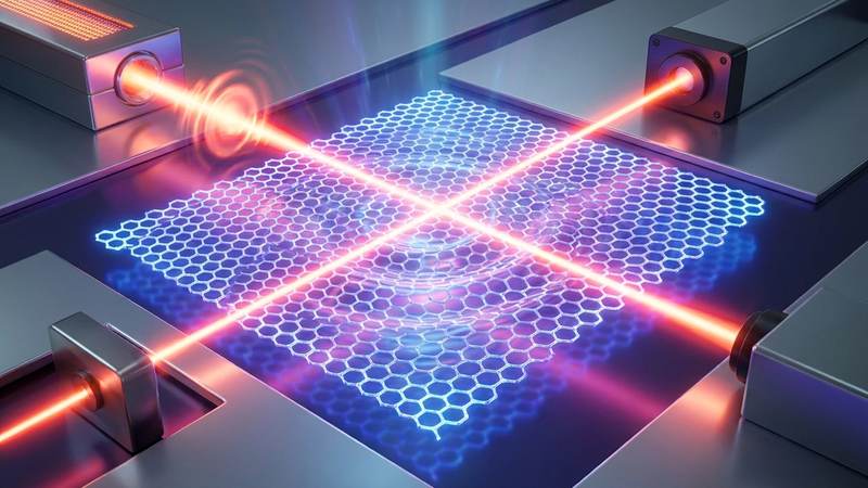
To understand why graphene is so exceptionally suited for terahertz applications, one must first examine its unique band structure, where charge carriers behave as massless Dirac fermions. Unlike conventional bulk semiconductors that exhibit parabolic energy-momentum dispersion, electrons and holes in graphene feature a linear dispersion relation near the Dirac points. This gapless nature implies that graphene can absorb photons of any energy, providing an inherently broadband optical response that encompasses the entire terahertz spectrum. When interacting with terahertz radiation, the intra-band transitions dominate the optical conductivity, which can be accurately described by the classical Drude model. By electrically or chemically tuning the Fermi level, researchers can drastically alter these intra-band dynamics, effectively modulating the material's opacity and refractive index in real time. This intrinsic tunability separates graphene from conventional optical materials, which typically require slow, power-hungry thermal or mechanical mechanisms to achieve similar modulation depths.
The tunability of graphene's optical conductivity is a direct consequence of the Pauli blocking principle, which governs the allowed energetic transitions of its charge carriers. When the Fermi level is shifted away from the Dirac point via an external gate voltage, low-energy inter-band transitions are forbidden because the final quantum states are already occupied. In the terahertz regime, this means that a simple field-effect transistor geometry can be utilized to toggle the material between highly transparent and highly absorptive states. Additionally, the extremely low density of states near the Dirac point ensures that even a small amount of injected charge yields a significant shift in the Fermi energy. This strong field effect is precisely what enables the creation of highly efficient, low-power terahertz modulators and active metamaterial devices. Engineers exploit this sensitivity to design optical switches that operate at gigahertz clock speeds with minimal energy dissipation.
Beyond simple Drude-like absorption, graphene also supports highly confined electromagnetic surface waves known as surface plasmon polaritons. In the terahertz and mid-infrared frequencies, these graphene plasmons exhibit extreme spatial confinement, squeezing light into volumes millions of times smaller than the free-space wavelength. This deep sub-wavelength confinement dramatically enhances the local electric field of the incident terahertz waves, facilitating exceptionally strong light-matter interactions even within a single atomic layer. The resonant frequency of these plasmons is dynamically tunable via electrostatic gating, offering an elegant mechanism for active spectral filtering and phase manipulation. Consequently, the integration of plasmonic nanostructures with graphene has emerged as a cornerstone strategy for enhancing the responsivity of terahertz photodetectors and the emission efficiency of terahertz sources. Harnessing these collective electronic oscillations allows researchers to manipulate light on a scale previously thought impossible by standard diffraction limits.
Ultrafast Carrier Dynamics and Nonlinear Optical Responses
The response of graphene to intense terahertz fields is governed by its ultrafast carrier dynamics, which dictate how energy is absorbed, distributed, and dissipated within the lattice. Upon the absorption of a terahertz photon, an electron is excited to a higher energy state, creating a non-equilibrium distribution of charge carriers. Because electron-electron scattering in graphene is exceptionally fast, occurring on a femtosecond timescale, these photoexcited carriers rapidly thermalize to form a hot carrier gas. The temperature of this hot electron gas can significantly decouple from the underlying atomic lattice due to the relatively weak electron-phonon interaction at these energy scales. This localized heating effect is highly advantageous for optoelectronic applications, as it forms the physical basis for highly sensitive photothermoelectric and bolometric terahertz detection mechanisms. Capturing this transient thermal energy before it dissipates is the primary engineering challenge in modern detector design.
Following the initial thermalization process, the hot carriers must eventually cool down and transfer their energy to the lattice via the emission of optical and acoustic phonons. In pristine graphene, optical phonon emission is highly efficient but requires the electrons to possess an energy greater than the optical phonon energy threshold of approximately two hundred milli-electron volts. Since typical terahertz photons carry energies of only a few milli-electron volts, cooling must predominantly occur through highly inefficient acoustic phonon scattering or defect-mediated pathways. This slow cooling bottleneck essentially prolongs the lifetime of the hot carrier state, thereby enhancing the magnitude of the photo-induced voltage or current in detector geometries. Understanding and engineering these relaxation pathways is therefore critical for optimizing the speed and sensitivity of graphene-based terahertz devices. By manipulating the substrate and defect density, scientists can artificially tailor these cooling rates to suit specific application requirements.
The unique band structure and ultrafast thermalization dynamics of graphene also give rise to extraordinary nonlinear optical properties under intense terahertz irradiation. Because the velocity of Dirac fermions is constant and independent of their momentum, their acceleration in an oscillating electromagnetic field is inherently nonlinear. This results in a massive third-order nonlinear susceptibility, enabling highly efficient high-harmonic generation and frequency multiplication processes directly within the terahertz band. Furthermore, saturable absorption can be easily achieved at relatively low incident fluences, making graphene an excellent passive mode-locker for terahertz quantum cascade lasers. The ability to manipulate these nonlinear responses through electrostatic gating provides a powerful tool for developing active optical components required for advanced terahertz communication protocols. Exploiting these extreme non-linearities paves the way for all-optical signal processing and advanced spectroscopic techniques.
Engineering Graphene-Based Terahertz Photodetectors
Detecting terahertz radiation with high sensitivity and speed at room temperature has been one of the most persistent challenges in modern applied physics. Graphene has emerged as a revolutionary material for this purpose, supporting multiple distinct physical mechanisms for converting terahertz photons into measurable electrical signals. The most prominent among these is the photothermoelectric effect, which relies on the generation of a temperature gradient between the active graphene channel and the metal contacts. Because graphene possesses a highly tunable Seebeck coefficient, an asymmetric junction can be created by locally gating the material or utilizing dissimilar contact metals. When the hot carrier gas is generated by incident terahertz radiation, this asymmetry drives a net thermoelectric current that is directly proportional to the incident optical power. This self-powered detection scheme circumvents the need for external bias voltages, thereby eliminating a major source of electrical dark noise.
Another dominant detection mechanism in the terahertz regime is the plasma-wave rectification effect, historically described by the Dyakanov-Shur theory. In a graphene field-effect transistor with a sub-micron channel length, the electron liquid can support propagating plasma waves that are excited by the incoming alternating electric field. Due to the inherent nonlinearities in the device transport equations, these high-frequency plasma oscillations are rectified into a steady direct-current drain-to-source voltage. Graphene is particularly well-suited for this mechanism because its high carrier mobility ensures that the plasma waves undergo minimal damping before reaching the contacts. This allows the devices to operate in the resonant detection regime, offering highly tunable, frequency-selective detection of terahertz signals well beyond the conventional transit-time cutoff frequencies. Designing the channel geometry to match specific plasma resonances is crucial for maximizing the responsivity of these sophisticated detectors.
The ultimate performance metric for any photodetector is its noise equivalent power, which quantifies the minimum detectable signal against the intrinsic electrical noise of the device. Graphene photodetectors have demonstrated exceptional noise equivalent power figures, often rivaling or surpassing those of commercially available cryogenic bolometers, while operating entirely at room temperature. To achieve these low noise floors, engineers must carefully manage the thermal noise by minimizing the device resistance and suppressing dark currents through optimal contact engineering. Furthermore, the integration of external antenna structures, such as bow-tie or log-periodic antennas, is routinely employed to overcome the low optical absorption of single-layer graphene. By funneling the macroscopic terahertz beam into the deep sub-wavelength active area of the graphene channel, these antennas dramatically boost the responsivity and overall signal-to-noise ratio. The seamless integration of micro-antennas with two-dimensional active regions remains a focal point for current commercialization efforts.
Terahertz Modulators and Spatial Manipulators
The ability to dynamically manipulate the amplitude, phase, and polarization of a terahertz beam is essential for applications ranging from high-speed wireless communications to advanced computational imaging. Graphene operates as an exceptional active medium for these modulators due to the broadband tunability of its complex optical conductivity via the field effect. By incorporating graphene into an optical cavity or a waveguide structure, a small modulation of the gate voltage translates into a massive change in the transmission or reflection coefficient of the device. This electro-absorption modulation can occur at gigahertz speeds, limited primarily by the parasitic resistance and capacitance of the external driving circuit rather than the intrinsic carrier dynamics. Consequently, graphene-based amplitude modulators currently represent the state of the art for encoding digital information onto terahertz carrier waves. Their low insertion loss and high modulation depth make them ideal candidates for integration into next-generation telecommunication transmitters.
To achieve deeper modulation depths and phase manipulation, researchers frequently couple graphene with engineered periodic structures known as metamaterials or metasurfaces. A typical terahertz metasurface consists of an array of sub-wavelength metallic resonators, such as split-ring resonators, fabricated directly on top of a graphene sheet. These metallic structures exhibit strong electromagnetic resonances that localize the terahertz electric field tightly within the adjacent graphene layer, thereby magnifying the light-matter interaction. By tuning the Fermi level of the graphene, the damping rate of the metasurface resonance is dynamically altered, shifting both its spectral position and its quality factor. This hybrid approach allows for near-perfect amplitude modulation, as well as an active control over the phase front of the transmitted or reflected terahertz wave. The synthesis of metasurface physics with tunable two-dimensional materials has drastically expanded the design space for flat optics.
Beyond single-pixel modulators, the spatial manipulation of terahertz light is actively being explored through the development of graphene-based spatial light modulators. By patterning the gate electrodes into an individually addressable two-dimensional array, the optical properties of the graphene sheet can be spatially varied across the aperture of the device. This capability enables the generation of complex holographic projections, dynamic beam steering, and adaptive optics in the terahertz frequency range. The transition from rigid substrates to flexible polymers has further expanded the utility of these spatial light modulators, allowing them to be conformed to curved surfaces for wearable electronics or non-destructive testing applications. As manufacturing techniques for large-area chemical vapor deposition graphene continue to mature, the scalability and resolution of these active terahertz arrays will inevitably improve. This precise spatial control is the missing link for developing high-resolution, real-time terahertz imaging cameras.
Engineering Terahertz Sources and Emitters
While detection and modulation technologies have seen rapid commercialization, the realization of efficient, room-temperature terahertz sources remains the most formidable challenge in the field. Graphene offers several intriguing pathways for the generation of terahertz radiation, primarily leveraging its unique plasmonic properties and highly non-equilibrium carrier distributions. One promising approach involves the continuous-wave optical pumping of graphene to achieve a population inversion between the electron and hole states in the Dirac cone. If the recombination pathways are carefully engineered, this inverted state can theoretically stimulate the emission of terahertz photons, acting as a two-dimensional gain medium for novel laser architectures. Although achieving a sustained continuous-wave population inversion is incredibly difficult due to the ultrafast thermalization rates, significant progress is being made using pulsed excitation schemes. Exploring intricate cavity designs to lower the threshold for stimulated emission is currently a major focus of theoretical and experimental research.
Another highly researched mechanism for terahertz generation in graphene relies on the excitation of high-momentum surface plasmons and their subsequent conversion into free-space radiation. When a direct electrical current is driven through a high-mobility graphene channel, the drifting charge carriers can interact with the fundamental plasmon modes of the structure. Under certain boundary conditions, an instability known as the Dyakonov-Shur instability occurs, causing the plasma waves to grow exponentially and radiate electromagnetic energy at terahertz frequencies. To extract this energy efficiently, metallic grating structures or acoustic cavities must be integrated to provide the necessary momentum matching between the slow-moving plasmons and the fast-moving free-space photons. This electrically driven, solid-state emission paradigm holds the potential to yield compact, tunable, and continuous-wave terahertz sources that bypass the limitations of traditional semiconductor oscillators. Harnessing these hydrodynamic electron flows represents a radical departure from conventional laser physics.
Graphene is also being heavily utilized as an integrated nonlinear medium for the generation of terahertz radiation via difference frequency generation and optical rectification. By illuminating the material with two distinct near-infrared or mid-infrared laser beams, the strong third-order nonlinearity of the Dirac fermions facilitates the generation of a beat frequency that falls squarely within the terahertz gap. This process is particularly efficient when enhanced by the aforementioned plasmonic metasurfaces, which relax the strict phase-matching conditions typically required in bulk nonlinear crystals. The resulting terahertz pulses are inherently phase-locked to the driving lasers, making them highly suitable for time-domain spectroscopy and coherent control experiments. As the understanding of graphene's nonlinear tensor elements deepens, optimizing the efficiency of these frequency down-conversion techniques will become a major focus for ultrafast science. The ability to generate broadband terahertz pulses from an atomically thin layer is an unprecedented achievement in non-linear optics.
Integration with Hybrid Material Platforms
The true technological potential of graphene is fully realized only when it is integrated with other advanced material platforms to form hybrid, multifunctional optoelectronic systems. Because graphene is held together by strong in-plane covalent bonds but lacks out-of-plane dangling bonds, it can be transferred onto virtually any substrate without suffering from the lattice-mismatch constraints that plague traditional epitaxy. The advent of van der Waals heterostructures, where graphene is stacked with other two-dimensional materials like hexagonal boron nitride or transition metal dichalcogenides, has been particularly revolutionary. Encapsulating graphene within atomically flat layers of hexagonal boron nitride shields it from environmental impurities and substrate scattering, thereby preserving its ultra-high intrinsic carrier mobility. This pristine environment is absolutely crucial for maintaining the long plasmon lifetimes and long mean free paths required for coherent terahertz device operation. Building these atomic-scale LEGO structures allows engineers to design artificial materials with bespoke electronic and optical properties.
Integration with established semiconductor photonics is equally important for the commercial viability of graphene-based terahertz technologies. Researchers have successfully coupled graphene with silicon waveguides, gallium arsenide quantum cascade lasers, and complementary metal-oxide-semiconductor read-out integrated circuits. For instance, incorporating a graphene layer onto the facet of a terahertz quantum cascade laser allows for the active stabilization, Q-switching, or mode-locking of the laser output through purely electronic means. This hybrid integration strategy leverages the immense manufacturing infrastructure of the silicon industry while simultaneously injecting the unprecedented broadband optoelectronic capabilities of two-dimensional materials. As wafer-scale transfer techniques become more reliable, the seamless integration of graphene into standard foundry processes will catalyze the mass production of next-generation terahertz microchips. Bridging the gap between exotic nanomaterials and standardized industrial manufacturing is the ultimate key to widespread adoption.
FAQ
What exactly is the terahertz gap and why is it so difficult to bridge? The terahertz gap refers to the portion of the electromagnetic spectrum between microwave and infrared frequencies, typically spanning from one to ten terahertz. It has been historically difficult to bridge because conventional electronic transistors are too slow to oscillate at these frequencies due to transit-time limitations. Simultaneously, traditional photonic devices like semiconductor lasers suffer from severe thermal noise and non-radiative recombination losses at such low photon energies. Graphene bridges this gap because its massless Dirac fermions provide an ultra-fast electronic response combined with a gapless, broadband optical absorption profile. This dual nature allows it to operate efficiently at the exact intersection of electronics and photonics.
How does graphene detect terahertz radiation at room temperature? Graphene detects terahertz radiation primarily through the photothermoelectric effect and the plasma-wave rectification mechanism. When incident terahertz light strikes the material, it rapidly heats the charge carriers, creating a hot electron gas that is thermally decoupled from the atomic lattice. If the device features an asymmetric contact geometry or a localized gate field, this temperature gradient drives a measurable thermoelectric current. Alternatively, the alternating electric field of the terahertz wave can excite plasma oscillations in the electron liquid, which are then rectified into a direct current by the inherent nonlinearities of the device. Both mechanisms are highly efficient at room temperature, eliminating the need for bulky cryogenic cooling systems.
What role do plasmonics play in graphene terahertz devices? Plasmonics play a critical role by artificially enhancing the strength of the interaction between the terahertz light and the single atomic layer of graphene. Because a monolayer of graphene absorbs only a small fraction of incident light, metallic antennas or resonant metasurfaces are patterned nearby to concentrate the electromagnetic field. These structures excite surface plasmon polaritons, which squeeze the long-wavelength terahertz radiation into deep sub-wavelength volumes right at the graphene interface. This massive field enhancement directly translates to higher responsivity in photodetectors and deeper modulation depths in active optical filters. Furthermore, the resonant frequency of these plasmons can be dynamically tuned by altering the gate voltage applied to the graphene.
Can graphene be used to build a continuous-wave terahertz laser? Building a continuous-wave terahertz laser from graphene remains a highly theoretical and exceptionally challenging endeavor for the scientific community. The primary obstacle is the incredibly fast thermalization rate of the charge carriers, which prevents the establishment of a stable population inversion required for stimulated emission. However, researchers are exploring alternative emission mechanisms, such as exploiting the Dyakonov-Shur instability to convert drifting direct-current plasma waves into radiating terahertz photons. Another heavily researched avenue is utilizing graphene as a highly efficient nonlinear medium to generate terahertz waves through the difference frequency mixing of two optical laser beams. While a standalone graphene laser is not yet realized, its use as an active component in hybrid terahertz sources is highly successful.
How does the integration of hexagonal boron nitride improve graphene devices? Hexagonal boron nitride is an insulating, two-dimensional material that features an atomically flat surface devoid of dangling bonds or charge traps. When graphene is placed directly onto standard substrates like silicon dioxide, the surface roughness and trapped impurities severely scatter the charge carriers, degrading the material's performance. Encapsulating the graphene between layers of hexagonal boron nitride shields the Dirac fermions from these external perturbations, allowing the material to achieve its theoretical limit of carrier mobility. This high mobility is essential for terahertz applications because it minimizes resistive losses, maximizes the plasmon lifetime, and enables the observation of advanced hydrodynamic electron transport. Consequently, this encapsulation technique is now the gold standard for fabricating high-performance terahertz optoelectronics.
Conclusion
The comprehensive exploration of graphene's optoelectronic properties has unequivocally established it as the premier platform for engineering the next generation of terahertz technologies. From the fundamental physics of massless Dirac fermions to the intricate design of plasmonic metasurfaces, the manipulation of low-energy photons has been forever transformed by this two-dimensional carbon lattice. The successful demonstration of room-temperature photodetectors, gigahertz-speed modulators, and hybrid quantum cascade laser architectures represents merely the initial phase of this technological revolution. As researchers continue to refine large-scale fabrication techniques and push the boundaries of van der Waals heterostructures, the commercial barriers to entry for terahertz systems will rapidly diminish. Ultimately, this will unlock unprecedented capabilities in quantum science, medical imaging, non-destructive material inspection, and ultra-high-bandwidth wireless communications. The foundational principles reviewed here will serve as the guiding light for decades of future engineering endeavors.
Looking forward, the true disruption will likely emerge from the seamless integration of graphene-based terahertz components into existing semiconductor ecosystems. The ability to deposit highly active, tunable optical materials directly atop complementary metal-oxide-semiconductor electronics paves the way for monolithic, multi-spectral system-on-chip architectures. As the demand for data transfer rates pushes communication networks into the sixth-generation standards and beyond, the terahertz carrier frequencies enabled by these devices will become indispensable. The foundational work reviewed by the scientific community provides the essential blueprint for navigating this complex but immensely rewarding frontier of applied physics. By mastering the intricate dance of electrons and photons within a single atomic plane, engineers are actively illuminating the darkest region of the electromagnetic spectrum. The terahertz gap, once a formidable obstacle, is steadily being closed by the remarkable properties of graphene.
Evaluate Our Quality
Serious about B2B integration? Test our premium Pulsed Electrical Resistive Carbon Heating turbostratic graphene in your lab. 100g sample packs available now.