Cryogenic Graphene Phase Modulators: A Theoretical Blueprint for Quantum Photonics
Researchers led by Leonard Barboza Navarro, Maria Carolina Volpato, Alisson Ronieri Cadore, and Pierre-Louis de Assis have conducted a study that systematically investigates the theoretical foundations of compact dual-layer graphene electro-optic phase modulators tailored for cryogenic quantum information processing. Photonic quantum computing relies heavily on the precise manipulation of quantum states using light, which necessitates components that operate with extreme efficiency at very low temperatures. Traditional electro-optic modulators often struggle to maintain their performance metrics when cooled to the cryogenic regimes required for quantum coherence, typically suffering from increased insertion losses or requiring unwieldy device footprints. The research team recognized that integrating two-dimensional materials with established silicon nitride waveguide platforms could overcome these fundamental limitations. By leveraging the unique tunable optical properties of graphene, their theoretical framework provides a clear pathway for developing next-generation quantum photonic integrated circuits. This rigorous analysis establishes a new paradigm for designing scalable hardware capable of supporting fault-tolerant quantum algorithms.
The integration of electro-optic modulators into fully cryogenic platforms is a critical bottleneck in the scaling of photonic quantum computers. Quantum information processing architectures demand hundreds or thousands of active components to route photons, perform logical operations, and manage quantum entanglement without destroying the fragile quantum states. Compactness and ultra-low insertion losses are absolute prerequisites for these components, as any photon loss directly translates to computational errors and reduced fidelity in quantum operations. Graphene has emerged as a highly promising material for electro-optic modulation due to its gate-tunable chemical potential and exceptionally broad spectral operating range. However, designing graphene-based devices that operate efficiently under the stringent constraints of cryogenic environments requires a deep understanding of solid-state physics and electromagnetic wave propagation. The theoretical models developed in this research directly address these complex multidisciplinary engineering challenges.
To address these multifaceted engineering challenges, the researchers employed advanced electromagnetic simulations coupled with a highly rigorous physical description of graphene conductivity. The theoretical investigation focuses specifically on dual-layer graphene structures, which offer enhanced interaction with the optical modes propagating through the underlying dielectric waveguides. Operating at cryogenic temperatures profoundly alters the electron dynamics within the graphene lattice, shifting the operational paradigm compared to room-temperature devices. The study highlights how these low-temperature environments can actually be leveraged to improve device metrics, rather than acting as a hindrance to electro-optic performance. This comprehensive analysis ultimately yields quantitative design guidelines that will inform the fabrication of scalable, low-loss quantum photonic networks. Engineers can use these guidelines to bypass the empirical guesswork traditionally associated with nanoscale device prototyping.
Achieving pure phase modulation without introducing unwanted amplitude modulation is notoriously difficult in conventional integrated photonics, especially when attempting to minimize the physical footprint of the device. The dual-layer graphene architecture proposed in this theoretical study directly tackles this challenge by exploiting the transition into the Pauli-blocking regime. Through careful optimization of the waveguide geometry and the intervening dielectric layers, the researchers demonstrated that it is possible to decouple phase modulation from absorption losses. The resulting optimized designs boast impressive theoretical performance metrics, including insertion losses well below a fraction of a decibel. These findings represent a significant leap forward in the quest to build practical, large-scale quantum computers based on integrated photonic technologies. The research proves that high-speed, compact phase modulation is theoretically achievable within strict cryogenic constraints.
The Imperative for Cryogenic Graphene Modulators in Quantum Photonics
Photonic quantum computing architectures require a highly controlled environment to preserve the delicate nature of single-photon states and entangled photon pairs. Superconducting nanowire single-photon detectors, which are integral to reading out quantum states, strictly require cryogenic operating temperatures to function without excessive dark counts. Consequently, placing the entire photonic integrated circuit inside a dilution refrigerator simplifies the overall system architecture and minimizes thermal noise. This monolithic approach necessitates that all active optical components, including phase modulators, operate flawlessly at temperatures approaching absolute zero. Standard lithium niobate or silicon depletion modulators often exhibit altered carrier dynamics or increased driving voltage requirements when subjected to deep cryogenic cooling. This physical reality drives the urgent need for novel material platforms that thrive in extreme cold.
Graphene presents a highly attractive alternative for cryogenic electro-optic modulation due to its linear electronic band structure and lack of a bandgap. The optical conductivity of graphene can be dynamically controlled by applying an external electric field, which shifts the Fermi level and alters the probability of interband electronic transitions. At room temperature, thermal broadening of the electron distribution blurs the sharp transition between absorbing and transparent states, requiring larger voltage swings to achieve significant modulation. Cryogenic environments naturally suppress this thermal broadening, thereby sharpening the Fermi-Dirac distribution and enhancing the electro-optic response of the material. This temperature-dependent behavioral shift is precisely what makes graphene an ideal candidate for low-power, high-efficiency quantum photonic modulators. The material essentially becomes more cooperative and efficient as the ambient temperature drops.
Integrating these two-dimensional materials with silicon nitride waveguides offers a highly scalable platform for quantum information processing. Silicon nitride is renowned for its ultra-low optical propagation losses across a broad range of wavelengths, making it the material of choice for passive quantum photonic routing. By depositing dual-layer graphene heterostructures directly onto these low-loss waveguides, engineers can create active tuning elements without significantly perturbing the optical mode. The evanescent field of the light traveling through the silicon nitride core interacts strongly with the overlying graphene layers, enabling efficient phase accumulation over very short propagation distances. This strong light-matter interaction is crucial for reducing the overall device footprint, which directly impacts the number of components that can be packed onto a single cryogenic chip. A smaller footprint directly correlates to higher qubit density and processing power.
The primary challenge in designing these hybrid structures lies in balancing the required phase shift against the optical absorption inherently introduced by the graphene layers. In quantum photonics, any absorption event constitutes a lost photon, which is catastrophic for deterministic quantum logic operations. Therefore, the modulator must operate in a regime where the real part of the effective refractive index changes significantly while the imaginary part remains vanishingly small. Achieving this delicate balance requires precise control over the graphene Fermi level, the quality of the material, and the spatial overlap between the optical mode and the two-dimensional electron gas. The theoretical framework developed in this study provides the necessary computational tools to navigate this complex multidimensional optimization problem. The resulting parameter maps act as a definitive guide for future experimental implementations.
Theoretical Framework and the Kybo Formalism
Accurately modeling the optical response of graphene across different temperatures and chemical potentials requires a physically rigorous mathematical framework. The researchers utilized the Kybo formalism to describe the complex surface conductivity of the graphene layers within their electromagnetic simulations. This theoretical approach goes beyond simple Drude models by accurately capturing both intraband electron scattering and interband transition phenomena under finite temperature conditions. The Kybo formalism is particularly vital for cryogenic simulations because it correctly accounts for the energy-dependent scattering rates and the exact shape of the Fermi-Dirac distribution. By integrating this advanced conductivity model into their simulation suite, the team could predict the optical behavior of the modulators with unprecedented theoretical accuracy. This accuracy is essential for identifying the narrow operational windows where pure phase modulation occurs.
The complex surface conductivity of graphene dictates how the material interacts with the oscillating electromagnetic field of the guided optical mode. The real part of the conductivity governs the absorption of light through interband transitions and free-carrier scattering, directly contributing to insertion loss. Conversely, the imaginary part of the conductivity influences the phase velocity of the optical wave, enabling the desired electro-optic phase modulation. The Kybo formalism allows researchers to map out these conductivity components as a continuous function of the applied gate voltage and the ambient temperature. This high-resolution mapping is essential for identifying the precise operating points where phase modulation is maximized and optical absorption is effectively suppressed. Such detailed theoretical mapping prevents costly trial-and-error iterations during the physical fabrication phase.
Electromagnetic simulations utilizing this rigorous conductivity model reveal complex interactions between the dual graphene layers and the confined silicon nitride optical mode. As the applied voltage alters the carrier density in the top and bottom graphene sheets, the effective refractive index of the composite waveguide structure undergoes a subtle but highly impactful shift. The finite-element method simulations employed by the research team calculate the eigenmodes of the waveguide cross-section for various electrostatic biasing conditions. These calculations extract both the effective mode index and the propagation loss, which are the two fundamental metrics defining modulator performance. The accuracy of these finite-element computations is directly tied to the physical fidelity of the underlying Kybo surface conductivity model. Without this rigorous foundation, any simulated performance metrics would be highly suspect and unreliable.
A critical aspect of the theoretical modeling involves accurately representing the electrostatic field distribution within the dual-layer graphene capacitor structure. The two graphene sheets are separated by a thin dielectric spacer, forming a nanoscale parallel-plate capacitor that controls the carrier concentration. The simulations must self-consistently solve the Poisson equation to determine the exact Fermi level shift in each graphene layer for a given applied voltage. The quantum capacitance of graphene, which becomes highly relevant at low carrier densities, is intrinsically factored into these electrostatic calculations. This comprehensive theoretical approach ensures that the predicted modulation efficiencies and required driving voltages are grounded in realistic physical constraints. It proves that the proposed devices can operate within the voltage limits of standard cryogenic control electronics.
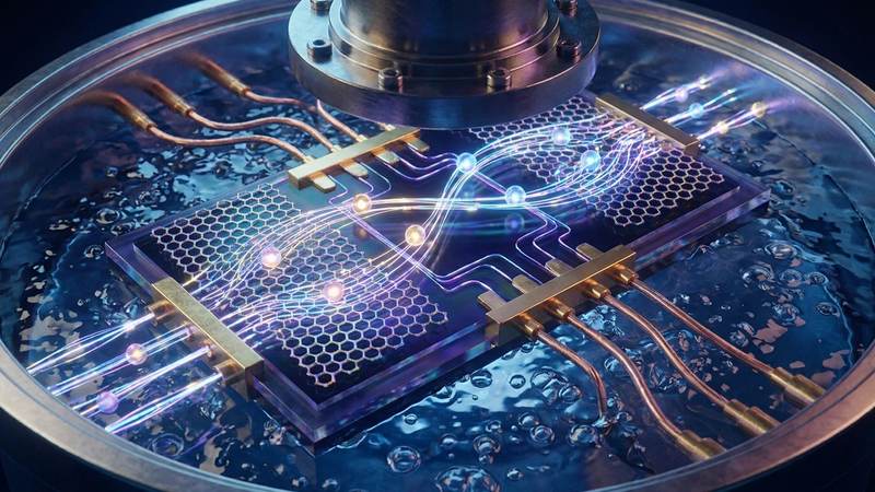
Dual-Layer Graphene Architecture on Silicon Nitride Waveguides
The dual-layer graphene configuration represents a sophisticated evolution in the design of two-dimensional electro-optic devices. In this architecture, two distinct monolayers of graphene are vertically stacked and separated by a high-quality dielectric material. This configuration acts as a highly efficient capacitor, where one layer serves as the active modulation medium and the other acts as a transparent top gate. Unlike single-layer designs that require bulky metallic gate electrodes near the optical mode, the dual-layer approach minimizes parasitic metallic absorption. The entire active region remains optically transparent, allowing the evanescent field of the underlying silicon nitride waveguide to interact purely with the tunable two-dimensional electron gas. This elegant geometry is fundamental to achieving the ultra-low insertion losses demanded by quantum applications.
Silicon nitride provides an optimal passive platform for this active dual-layer architecture due to its favorable optical and thermal properties. The moderate refractive index contrast of silicon nitride allows for strong optical confinement while maintaining a significant evanescent tail that penetrates into the graphene layers. Furthermore, silicon nitride exhibits exceptionally low intrinsic material absorption in the near-infrared spectrum, which is the standard operating wavelength for many quantum communication protocols. The material is also highly compatible with standard complementary metal-oxide-semiconductor fabrication processes, ensuring that the theoretical designs can be readily translated into physical prototypes. The thermal expansion coefficient of silicon nitride also aligns well with cryogenic cooling cycles, preventing mechanical delamination of the two-dimensional heterostructures. This thermomechanical stability is crucial for long-term reliability in dilution refrigerators.
The spatial overlap between the optical mode and the graphene layers is a critical design parameter that dictates the modulation efficiency. If the graphene is placed too far from the waveguide core, the light-matter interaction is weak, necessitating excessively long devices to accumulate a meaningful phase shift. Conversely, placing the graphene directly on the core maximizes interaction but can introduce unwanted scattering losses due to surface roughness or material defects. The researchers meticulously analyzed various waveguide geometries, including the core width and thickness, to optimize the evanescent field distribution. This geometric tuning ensures that the optical mode experiences the maximum possible change in effective index for a given shift in the graphene Fermi level. The resulting optimized geometries strike a perfect balance between interaction strength and passive propagation loss.
The dual-layer configuration also provides a unique advantage in terms of electrostatic symmetry and carrier injection. By applying a differential voltage across the two layers, equal and opposite charge densities are induced in the top and bottom sheets. This symmetric doping profile ensures that both layers contribute to the electro-optic phase shift simultaneously, effectively doubling the modulation efficiency compared to single-layer devices. Furthermore, the absence of a bulky metallic gate significantly reduces the parasitic capacitance of the structure, which is vital for achieving high-speed operation. The theoretical models confirm that this symmetric, metal-free active region is instrumental in reaching the stringent performance targets required for quantum information processing. It represents a highly optimized synergy between electrostatic control and optical waveguide design.
Pauli-Blocking and Fermi-Dirac Sharpening at Cryogenic Temperatures
The physical mechanism enabling low-loss phase modulation in graphene relies on a quantum mechanical phenomenon known as Pauli-blocking. In pristine, undoped graphene, incident photons with sufficient energy can excite electrons from the valence band to the conduction band, resulting in strong optical absorption. However, when an external electric field shifts the Fermi level beyond half the photon energy, these interband transitions are strictly forbidden by the Pauli exclusion principle. Once this critical doping threshold is crossed, the graphene layer suddenly becomes highly transparent to the incident optical mode. Operating the modulator deep within this Pauli-blocked regime is absolutely essential for minimizing insertion losses in quantum photonic circuits. The theoretical study meticulously maps the voltage required to sustain this transparent state.
Temperature plays a dominant role in determining the sharpness and effectiveness of the Pauli-blocking transition. At room temperature, the Fermi-Dirac distribution is thermally smeared, meaning that electron energy states are probabilistically occupied over a wide energy range. This thermal smearing causes residual interband absorption even when the nominal Fermi level is pushed well beyond the ideal Pauli-blocking threshold. To overcome this residual room-temperature absorption, engineers must apply excessively high gate voltages to push the Fermi level to extreme values. These high voltages can lead to dielectric breakdown or introduce excessive free-carrier absorption, ultimately limiting the performance of the phase modulator. The thermal noise essentially fights against the desired electro-optic switching mechanism.
Cooling the device to deep cryogenic temperatures, specifically around ten Kelvin, fundamentally alters this thermodynamic landscape. At these ultralow temperatures, the thermal energy available to the electrons is drastically reduced, causing the Fermi-Dirac distribution to become nearly a sharp step function. This sharpening implies that the transition between the absorbing state and the transparent Pauli-blocked state occurs over a much narrower range of applied voltages. Consequently, the modulator can achieve near-perfect transparency at significantly lower Fermi levels and lower driving voltages. The theoretical investigation demonstrates that this cryogenic enhancement is a massive advantage, enabling access to highly efficient operating regimes that are physically impossible at room temperature. The extreme cold acts as an operational catalyst rather than an environmental hurdle.
The sharpened Fermi-Dirac distribution at cryogenic temperatures also enhances the rate of change of the effective refractive index with respect to the applied voltage. Because the transition into the Pauli-blocked state is highly abrupt, the imaginary part of the graphene conductivity undergoes a rapid variation over a small voltage window. This rapid variation translates directly into a massive enhancement of the electro-optic phase modulation efficiency. The researchers leveraged this low-temperature phenomenon to dramatically reduce the required active length of the modulator while maintaining the necessary phase accumulation. This reduction in device footprint is a direct consequence of the unique interplay between quantum statistics and cryogenic environments. It highlights the profound benefits of co-designing the photonic hardware specifically for the dilution refrigerator environment.
Optimization of Dielectric Spacers and Waveguide Geometry
The dielectric spacer separating the two graphene layers is a seemingly passive component that actually dictates the entire electrostatic performance of the modulator. The thickness and relative permittivity of this spacer material determine the specific capacitance of the dual-layer structure. A higher specific capacitance allows for a larger induced carrier density in the graphene layers for a given applied gate voltage. However, reducing the spacer thickness to increase capacitance can lead to an increased risk of quantum tunneling or catastrophic dielectric breakdown under strong electric fields. The theoretical study carefully navigates these trade-offs to identify the optimal spacer parameters for safe and efficient cryogenic operation. The material choice here is just as critical as the graphene itself.
Hexagonal boron nitride is frequently utilized as the dielectric spacer of choice in high-quality graphene heterostructures. This material provides an atomically smooth interface that preserves the exceptional electron mobility of the adjacent graphene layers. High carrier mobility is crucial for minimizing intraband scattering losses, which become the dominant source of optical absorption once interband transitions are Pauli-blocked. The researchers incorporated the specific dielectric properties of hexagonal boron nitride into their electromagnetic and electrostatic simulations. By optimizing the thickness of this specific spacer material, they achieved a perfect balance between high capacitance and minimal defect-induced optical scattering. This specific material stack yields the highest theoretical performance margins for the modulator design.
Beyond the dielectric spacer, the geometry of the underlying silicon nitride waveguide requires meticulous optimization to maximize device performance. The width and height of the waveguide core determine the spatial distribution of the optical mode and its confinement factor. A highly confined mode reduces cross-talk between adjacent waveguides but minimizes the evanescent field available to interact with the graphene layers. Conversely, a weakly confined mode maximizes the light-matter interaction but increases the risk of radiation losses at waveguide bends. The systematic theoretical investigation explored a vast parameter space of waveguide dimensions to locate the exact geometric sweet spot for phase modulation. This exhaustive search ensures that the final design recommendations are globally optimal.
The position of the dual-layer graphene stack relative to the waveguide core also profoundly influences the modulation characteristics. The simulations revealed that introducing a thin buffer layer between the silicon nitride and the bottom graphene sheet can fine-tune the evanescent coupling. This buffer layer helps to mitigate potential scattering losses caused by surface roughness on the etched silicon nitride waveguide. By jointly optimizing the waveguide dimensions, the buffer layer thickness, and the properties of the intervening dielectric spacer, the researchers crafted a highly resilient device architecture. This holistic optimization approach ensures that the resulting modulator designs are both high-performing and robust against typical fabrication tolerances. It translates pure theoretical physics into practical, manufacturable engineering blueprints.
Balancing Insertion Loss and Modulation Length for Scalability
The ultimate metric of success for a quantum photonic phase modulator is its ability to deliver a required phase shift with the lowest possible insertion loss and physical footprint. The product of the voltage and the modulation length is a standard figure of merit used to evaluate the efficiency of electro-optic devices. In the context of fully integrated quantum computing, device footprints must be minimized to allow for the dense packing of hundreds of logical qubits and routing interferometers. The theoretical investigation demonstrates that the optimized cryogenic graphene modulators can achieve active modulation lengths below fifty micrometers. This extraordinary compactness is an order of magnitude smaller than many conventional lithium niobate devices utilized in similar quantum applications. Such miniaturization is critical for scaling up quantum processors.
Achieving this extremely short modulation length does not come at the expense of optical transmission efficiency. The researchers successfully identified operating regimes that simultaneously minimize the required device footprint and keep insertion losses strictly below a fraction of a decibel. Specifically, the optimized designs exhibit insertion losses below zero point three decibels at the targeted cryogenic temperature of ten Kelvin. This ultra-low loss metric is absolutely critical for maintaining the high fidelity required for generating and manipulating multi-photon entangled states. By operating deep within the Pauli-blocked regime enabled by the sharpened Fermi-Dirac distribution, the devices elegantly sidestep the traditional trade-off between size and absorption. They offer a rare win-win scenario in integrated photonic design.
Furthermore, the dual-layer graphene architecture inherently supports highly rapid electro-optic switching speeds. The ultimate bandwidth of the modulator is typically limited by the resistor-capacitor time constant of the device structure and its driving electronic circuitry. Because the active region is extremely short and devoid of massive metallic gate structures, the intrinsic capacitance remains remarkably low. The theoretical calculations confirm that these compact modulators can comfortably maintain operational bandwidths extending into the gigahertz scale. High-speed operation is essential for executing fast quantum logic gates and implementing real-time feed-forward error correction protocols in scalable quantum computers. This rapid responsiveness ensures the hardware can keep pace with advanced quantum algorithms.
The quantitative design guidelines produced by this systematic theoretical investigation provide a definitive roadmap for experimentalists and quantum engineers. By detailing the precise interplay between electrostatic tuning, material properties, and cryogenic physics, the study eliminates much of the empirical guesswork traditionally associated with device fabrication. The research establishes that near-pure phase modulation is not merely a theoretical curiosity, but an achievable engineering target within realistic voltage constraints. As the demand for scalable integrated quantum photonics continues to accelerate, these cryogenic graphene modulators represent a foundational technology for the next generation of computing architectures. The successful integration of these devices will undoubtedly propel the entire field of quantum information processing closer to fault-tolerant, large-scale commercial realization. It is a vital theoretical stepping stone toward practical quantum utility.
Frequently Asked Questions
What is the primary advantage of operating graphene phase modulators at cryogenic temperatures? Operating at cryogenic temperatures drastically reduces the thermal energy available to electrons within the graphene lattice. This lack of thermal energy causes the Fermi-Dirac distribution to sharpen into an abrupt step function. Because of this sharpening, the transition into the highly transparent Pauli-blocking regime occurs at significantly lower applied voltages. This allows the modulator to achieve near-perfect optical transparency and high phase efficiency without requiring extreme electrostatic driving fields. Ultimately, cryogenic cooling transforms the thermodynamic properties of graphene to vastly improve its electro-optic performance metrics.
How does the dual-layer graphene architecture differ from traditional single-layer designs? The dual-layer architecture utilizes two separate sheets of graphene separated by a thin, high-quality dielectric spacer. One layer acts as the active modulation medium while the second layer functions as a transparent electrostatic gate. This metal-free configuration eliminates the parasitic optical absorption normally caused by metallic electrodes placed near the waveguide core. By applying a differential voltage, equal and opposite charge densities are induced in both layers simultaneously. This symmetric dual-layer approach effectively doubles the light-matter interaction and significantly enhances the overall phase modulation efficiency.
Why is the Kybo formalism necessary for modeling these quantum photonic devices? The Kybo formalism provides a highly rigorous and physically consistent mathematical description of graphene surface conductivity. Unlike simplistic models, it accurately captures complex intraband scattering events and interband electron transitions across varying temperatures. This level of theoretical detail is strictly required to model the precise shape of the Fermi-Dirac distribution at ten Kelvin. Accurate conductivity modeling is essential for predicting the exact balance between optical phase accumulation and unwanted insertion losses. Without the Kybo formalism, the electromagnetic simulations would fail to accurately identify the high-efficiency Pauli-blocked operating regimes.
What specific performance metrics do the optimized cryogenic modulators achieve? The theoretical optimization identified device designs capable of exceptionally high performance under realistic voltage constraints. These optimized modulators achieve a near-pure phase modulation, minimizing any detrimental amplitude fluctuations during operation. The theoretical insertion losses are kept extremely low, strictly remaining below zero point three decibels at ten Kelvin. Furthermore, the required active modulation length is reduced to less than fifty micrometers, enabling highly compact device footprints. Despite this small size, the architecture maintains an intrinsic resistor-capacitor time constant that supports gigahertz-scale operational bandwidths.
Why is silicon nitride chosen as the underlying waveguide platform for these modulators? Silicon nitride is a widely adopted dielectric material in integrated photonics due to its extremely low intrinsic optical absorption. It exhibits an ultra-low propagation loss across the near-infrared spectrum, which is the standard wavelength range for many quantum optical applications. The material offers a moderate refractive index contrast that provides excellent optical confinement while maintaining a strong evanescent field. This strong evanescent tail is necessary to interact efficiently with the overlying dual-layer graphene heterostructure. Additionally, silicon nitride is highly compatible with standard semiconductor manufacturing processes and withstands deep cryogenic cooling without mechanical degradation.
Conclusion
The systematic theoretical investigation of dual-layer graphene electro-optic phase modulators establishes a highly promising paradigm for integrated quantum photonics. By rigorously modeling the complex interplay between electromagnetic wave propagation and cryogenic solid-state physics, the research team has unlocked new pathways for device optimization. The utilization of the Kybo formalism accurately highlighted the immense benefits of operating within the Pauli-blocked regime at ultralow temperatures. These cryogenic environments naturally suppress thermal electron smearing, sharpening the Fermi-Dirac distribution and enabling highly efficient phase modulation at reduced driving voltages. This fundamental shift in material behavior is the cornerstone of the proposed high-performance modulator architecture. The study proves that extreme cold is a critical asset for advanced electro-optic engineering.
The quantitative design guidelines derived from this study present a clear roadmap for realizing scalable, low-loss quantum computing components. By meticulously optimizing the waveguide geometry, dielectric spacer properties, and graphene quality, the models demonstrate that insertion losses can be suppressed below zero point three decibels. Achieving this ultra-low loss alongside active device lengths under fifty micrometers resolves a major bottleneck in the dense integration of photonic qubits. Furthermore, the capacity to maintain gigahertz-scale bandwidths ensures that these components can support the rapid logic operations demanded by fault-tolerant quantum algorithms. Ultimately, these cryogenic graphene modulators are poised to become indispensable building blocks in the ongoing evolution of advanced quantum information processing platforms. They represent a vital bridge between theoretical material science and practical quantum computing hardware.
Evaluate Our Quality
Serious about B2B integration? Test our premium Pulsed Electrical Resistive Carbon Heating turbostratic graphene in your lab. 100g sample packs available now.